特性
- Eight 0.7V HCSL differential output pairs
- Phase jitter: PCIe Gen3 < 1ps rms
- Phase jitter: PCIe Gen2 < 3.1ps rms
- Phase jitter: PCIe Gen1 < 86ps peak-to-peak
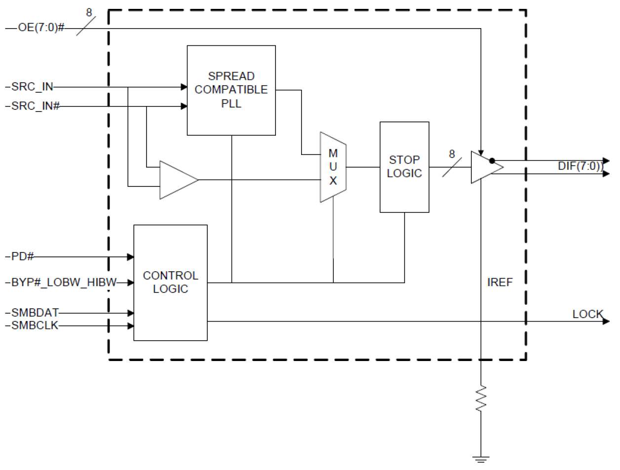
- Supports Zero Delay Buffer mode and Fanout mode
- Bandwidth programming available
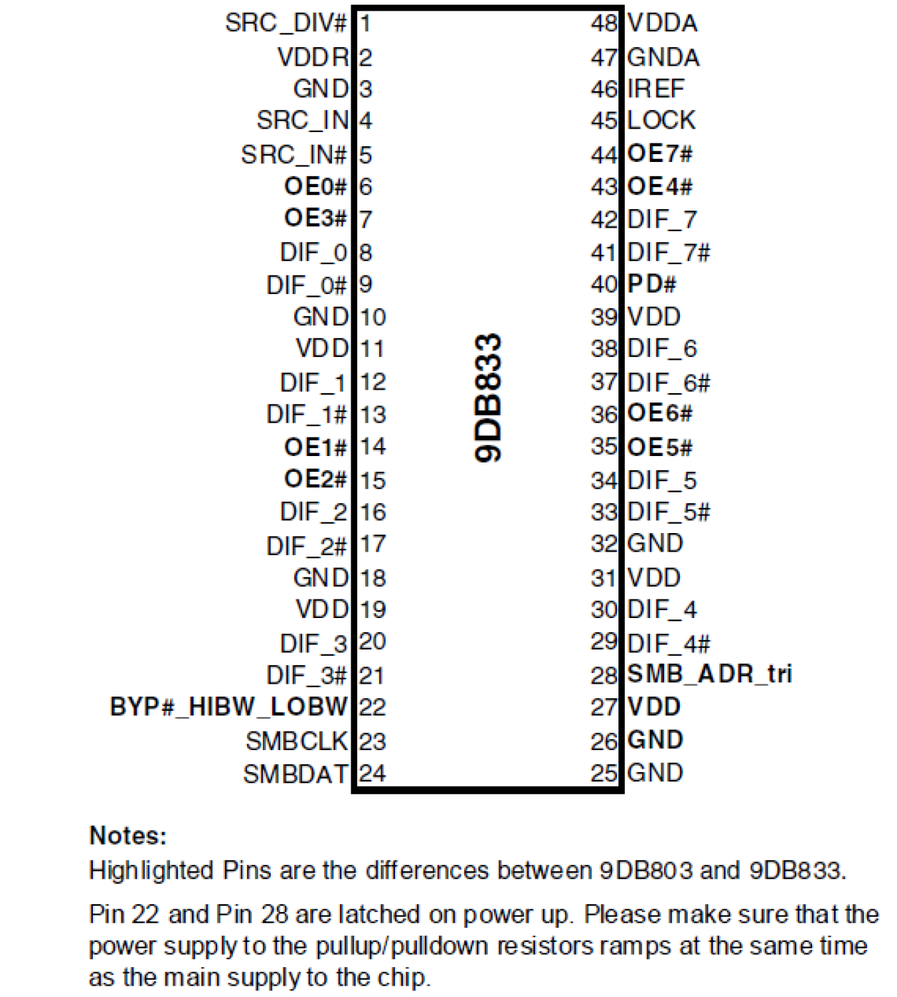
- 3 selectable SMBus Addresses
- 50MHz to 110MHz operation in PLL mode
- 5MHz to 166MHz operation in Bypass mode
描述
The 9DB833 zero delay buffer (ZDB) supports PCIe Gen3 requirements while being backward compatible with PCIe Gen2 and Gen1. The 9DB833 is driven by a differential SRC output pair from a 932S421 or 932SQ420 or equivalent main clock generator.
产品参数
| 属性 | 值 |
|---|---|
| Diff. Outputs | 8 |
| Diff. Output Signaling | HCSL |
| Output Freq Range (MHz) | 5 - 166.66 |
| Diff. Inputs | 1 |
| Diff. Input Signaling | HCSL |
| Accepts Spread Spec Input | Yes |
| Power Consumption Typ (mW) | 528 |
| Supply Voltage (V) | 3.3 - 3.3 |
| Output Type | HCSL |
| Diff. Termination Resistors | 32 |
| Package Area (mm²) | 76.3 |
| Battery Backup | No |
| Battery Seal | No |
| CPU Supervisory Function POR | No |
| Crystal Frequency Trimming | No |
| Frequency Out Pin | No |
| Inputs (#) | 1 |
| Input Freq (MHz) | 50 - 100 |
| Function | Zero Delay Buffer |
| Input Type | HCSL |
| Output Banks (#) | 1 |
| Core Voltage (V) | 3.3 |
| Output Voltage (V) | 0.8 |
| Product Category | PCI Express Clocks |
封装选项
| Pkg. Type | Pkg. Dimensions (mm) | Lead Count (#) | Pitch (mm) |
|---|---|---|---|
| TSSOP | 12.5 x 6.1 x 1.0 | 48 | 0.5 |
当前筛选条件


