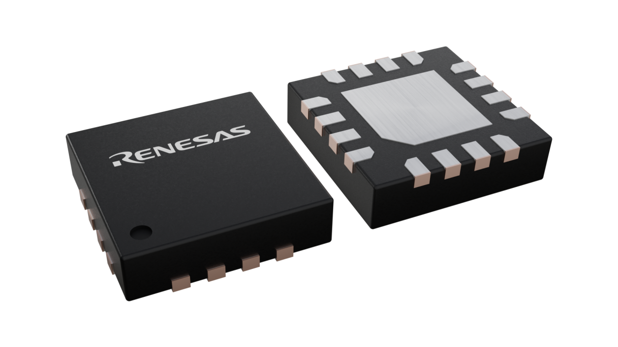
封装信息
| CAD 模型: | View CAD Model |
| Pkg. Type: | VFQFPN |
| Pkg. Code: | NLG16 |
| Lead Count (#): | 16 |
| Pkg. Dimensions (mm): | 3.0 x 3.0 x 1.0 |
| Pitch (mm): | 0.5 |
环境和出口类别
| Moisture Sensitivity Level (MSL) | 3 |
| Pb (Lead) Free | Yes |
| ECCN (US) | EAR99 |
| HTS (US) | 8542.39.0090 |
产品属性
| Lead Count (#) | 16 |
| Carrier Type | Tray |
| Moisture Sensitivity Level (MSL) | 3 |
| Qty. per Reel (#) | 0 |
| Qty. per Carrier (#) | 624 |
| Pb (Lead) Free | Yes |
| Pb Free Category | e3 Sn |
| Temp. Range (°C) | -40 to 85°C |
| Country of Assembly | MALAYSIA |
| Country of Wafer Fabrication | TAIWAN |
| Accepts Spread Spec Input | Yes |
| Advanced Features | Flexible Power Sequencing, Power Down Tolerant, Loss of Signal Indicator |
| App Jitter Compliance | PCIe Gen1, PCIe Gen2, PCIe Gen3, PCIe Gen4, PCIe Gen5 |
| Architecture | Common, SRNS, SRIS |
| Core Voltage (V) | 3.3V |
| Diff. Input Signaling | LP-HCSL |
| Diff. Inputs | 1 |
| Diff. Outputs | 2 |
| Diff. Termination Resistors | 0 |
| Feedback Input | No |
| Function | Fanout Buffer |
| Input Freq (MHz) | 10 - 220 |
| Input Type | HCSL, LVCMOS, LVDS, LVPECL |
| Inputs (#) | 1 |
| Length (mm) | 3 |
| MOQ | 624 |
| Output Banks (#) | 1 |
| Output Freq Range (MHz) | 10 - 220 |
| Output Impedance | 85 |
| Output Skew (ps) | 50 |
| Output Type | LP-HCSL |
| Output Voltage (V) | 3.3V |
| Outputs (#) | 2 |
| PLL | No |
| Package Area (mm²) | 16 |
| Pitch (mm) | 0.5 |
| Pkg. Dimensions (mm) | 3.0 x 3.0 x 1.0 |
| Pkg. Type | VFQFPN |
| Power Consumption Typ (mW) | 100 |
| Price (USD) | $1.8774 |
| Product Category | PCI Express Clocks |
| Prog. Clock | No |
| Reference Output | No |
| Spread Spectrum | Yes |
| Supply Voltage (V) | 3.3 - 3.3 |
| Tape & Reel | No |
| Thickness (mm) | 1 |
| Width (mm) | 3 |
有关 9DBL0255 的资源
描述
The 9DBL0255 device is a 2-output PCIe clock fanout buffer for PCIe Gen 1–7 applications. It has an open drain Loss of Signal (LOS) output to indicate the absence or presence of an input clock.
For information regarding evaluation boards and material, please contact your local sales representative.
