特性
- LP-HCSL outputs; save 18 resistors compared to standard HCSL outputs.
- 47 mW typical power consumption in PLL mode; minimal power consumption
- Separate power rail for LP-HCSL outputs can optionally be supplied from any voltage between 1.05 and 1.5 V; maximum power savings
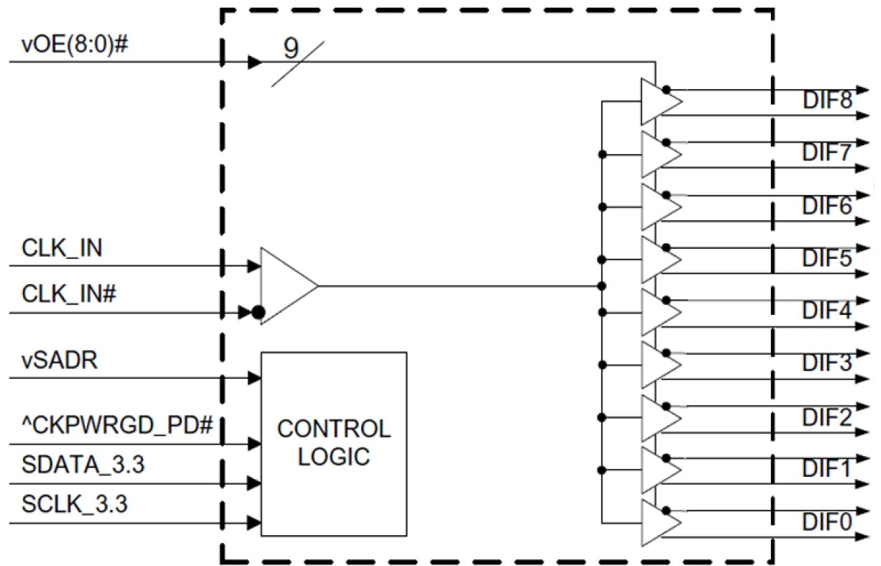
- OE# pin for each output; support DIF power management
- HCSL differential input; can be driven by common clock sources
- Spread spectrum tolerant; allows reduction of EMI
- Programmable Slew rate for each output; allows tuning for various line lengths
- Programmable output amplitude; allows tuning for various application environments
- 1 MHz to 167 MHz operating frequency
- Device contains default configuration; SMBus interface not required for device operation
- 3.3 V tolerant SMBus interface works with legacy controllers
- Selectable SMBus addresses; multiple devices can easily share an SMBus segment
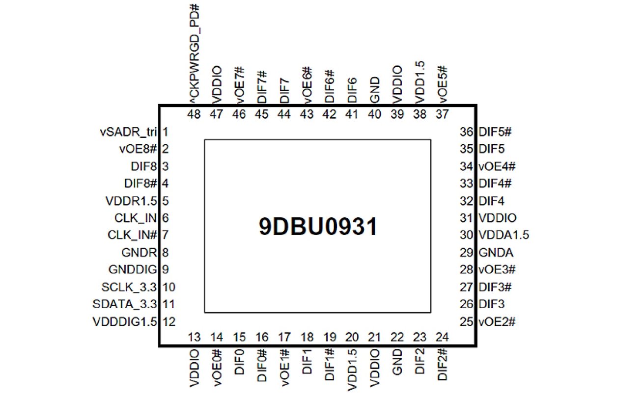
- Space-saving 6x6 mm 48-pin VFQFPN; minimal board space
描述
The 9DBU0931 is a member of IDT's 1.5 V Ultra-Low-Power (ULP) PCIe family. The device has 5 output enables for clock management, and 3 selectable SMBus addresses.
当前筛选条件


