
| CAD 模型: | View CAD Model |
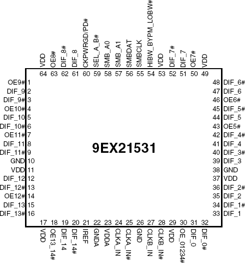
| Pkg. Type: | VFQFPN |
| Pkg. Code: | NLG64 |
| Lead Count (#): | 64 |
| Pkg. Dimensions (mm): | 9.0 x 9.0 x 0.9 |
| Pitch (mm): | 0.5 |
| Moisture Sensitivity Level (MSL) | 3 |
| Pb (Lead) Free | Yes |
| ECCN (US) | EAR99 |
| HTS (US) | 8542.39.0090 |
| Lead Count (#) | 64 |
| Carrier Type | Reel |
| Moisture Sensitivity Level (MSL) | 3 |
| Qty. per Reel (#) | 3000 |
| Qty. per Carrier (#) | 0 |
| Pb (Lead) Free | Yes |
| Pb Free Category | e3 Sn |
| Temp. Range (°C) | 0 to 70°C |
| Accepts Spread Spec Input | Yes |
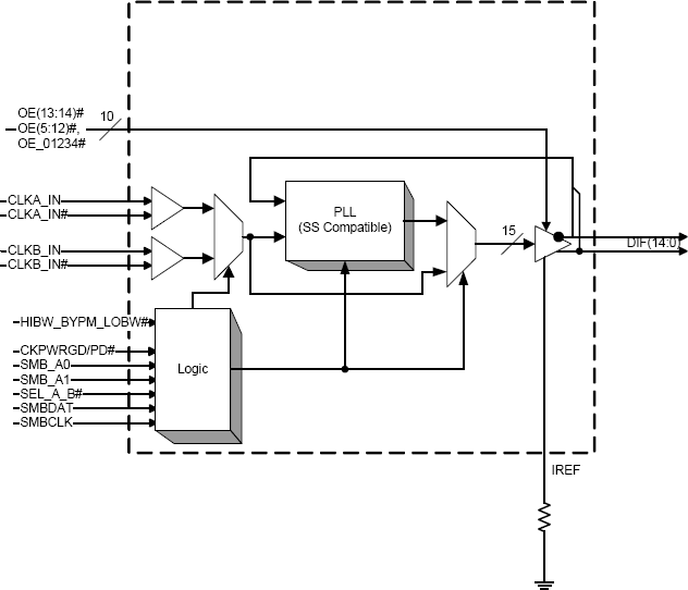
| Advanced Features | HW PLL mode control, Multiple SMBus addresses |
| App Jitter Compliance | PCIe Gen1, PCIe Gen2, PCIe Gen3, QPI |
| Architecture | Common, SRNS |
| C-C Jitter Max P-P (ps) | 50 |
| C-C Jitter Typ P-P (ps) | 20 |
| Core Voltage (V) | 3.3 |
| Diff. Input Signaling | HCSL |
| Diff. Inputs | 2 |
| Diff. Output Signaling | HCSL |
| Diff. Outputs | 15 |
| Diff. Termination Resistors | 60 |
| Feedback Input | No |
| Input Freq (MHz) | 166 |
| Input Type | HCSL |
| Inputs (#) | 2 |
| Length (mm) | 9 |
| MOQ | 3000 |
| Output Banks (#) | 1 |
| Output Freq Range (MHz) | 33.33 - 167 |
| Output Skew (ps) | 150 |
| Output Type | HCSL |
| Output Voltage (V) | 0.8 |
| Outputs (#) | 15 |
| PLL | Yes |
| Package Area (mm²) | 81 |
| Phase Jitter Max RMS (ps) | 1 |
| Phase Jitter Typ RMS (ps) | 0.6 |
| Pitch (mm) | 0.5 |
| Pkg. Dimensions (mm) | 9.0 x 9.0 x 0.9 |
| Pkg. Type | VFQFPN |
| Power Consumption Typ (mW) | 1089 |
| Prog. Clock | No |
| Prog. Interface | SMBUS |
| Reel Size (in) | 13 |
| Reference Output | No |
| Requires Terms and Conditions | Does not require acceptance of Terms and Conditions |
| Spread Spectrum | Yes |
| Supply Voltage (V) | 3.3 - 3.3 |
| Tape & Reel | Yes |
| Thickness (mm) | 0.9 |
| Width (mm) | 9 |
| 已发布 | No |
The 9EX21531 provides 15 output clocks for PCIe Gen1/ 2/3 applications. The 9EX21531 has 4 selectable SMBus addresses, and dedicated CKPWRGD/PD# and VDDA pins for easy board design. A differential clock from a CK410B+ or CK420BQ main clock generator, such as the 932S421, drives the 9EX21531. In fanout mode, the 9EX21531 provides outputs up to 166MHz.