特性
- Integrated terminations provide 100Ω differential Zo; reduced component count and board space
- 1.8V operation; reduced power consumption
- OE# pins; support DIF power management
- LP-HCSL differential clock outputs; reduced power and board space
- Programmable slew rate for each output; allows tuning for various line lengths
- Programmable output amplitude; allows tuning for various application environments
- DIF outputs are blocked until PLL is locked; clean system start-up
- Selectable 0%, -0.25% or -0.5% spread on DIF outputs; reduces EMI
- External 25MHz crystal; supports tight ppm with 0ppm synthesis error
- Configuration can be accomplished with strapping pins; SMBus interface is not required for device control
- 3.3V tolerant SMBus interface works with legacy controllers
- Space saving 5mm x 5mm 32-VFQFPN; minimal board space
- Selectable SMBus addresses; multiple devices can easily share an SMBus segment

9FGV0441 - Block Diagram
描述
The 9FGV0441 is a 4-output very-low power clock generator for PCIe Gen 1–4 applications with integrated output terminations providing Zo = 100Ω. The device has four output enables for clock management and supports two different spread spectrum levels in addition to spread off.
产品参数
| 属性 | 值 |
|---|---|
| Diff. Outputs | 4 |
| Diff. Output Signaling | LP-HCSL |
| Output Freq Range (MHz) | 25 - 25, 100 - 100 |
| Power Consumption Typ (mW) | 58 |
| Supply Voltage (V) | 1.8 - 1.8 |
| Output Type | LP-HCSL, LVCMOS |
| Xtal Freq (MHz) | 25 - 25 |
| Diff. Termination Resistors | 0 |
| Package Area (mm²) | 25 |
| Battery Backup | No |
| Battery Seal | No |
| CPU Supervisory Function POR | No |
| Crystal Frequency Trimming | No |
| Frequency Out Pin | No |
| Inputs (#) | 1 |
| Input Freq (MHz) | 25 - 25 |
| Function | Generator |
| Input Type | Crystal, LVCMOS |
| Core Voltage (V) | 1.8 |
| Output Voltage (V) | 0.8V, 1.8V |
| Product Category | PCI Express Clocks |
封装选项
| Pkg. Type | Pkg. Dimensions (mm) | Lead Count (#) | Pitch (mm) |
|---|---|---|---|
| VFQFPN | 5.0 x 5.0 x 0.9 | 32 | 0.5 |
应用方框图
 | RZ/G2E 电源和时序系统级模块 电源和时序系统级模块(SoM)确保精确的时序和高效的功率分配。 |
完成您的设计
寻找相关的产品,完善您的设计
Renesas Boards & Kits
RZ/N2H-EVKIT
有效
RZ/N2H 评估板套件
RZ/N2H 评估板套件是用于 RZ/N2H MPU 的一款评测和开发套件。 由于它具有板载仿真器,您只需将附带连线接到 PC 即可开始评测。 该评测板包含千兆以太网 PHY、非易失性存储器和 LPDDR4 存储器等功能丰富的元件,无需扩展板即可评估 RZ/N2H 的各种功能。
此外,通过扩展逆变器板,还可以实现多轴电机控制。
Partner Boards & Kits
SoM/SBC
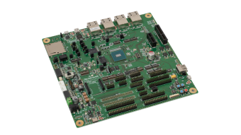
AP-RZV2-0A
Provides a CPU board equipped with the Renesas RZ/V2H. The RZ/V2H integrates a quad-core Arm® Cortex®-A55 with dual Arm® Cortex®-R8 cores, along with an AI accelerator and programmable hardware DRP, enabling fanless AI inference performance of up to 80 TOPS. Supports interfaces including Gigabit Ethernet, USB3.2 Gen2, M.2, microSD, MIPI CSI-2, and MIPI DSI, making it suitable for autonomous systems and FA machine vision applications requiring advanced AI processing.
Provided By:
AlphaProject Co.,Ltd.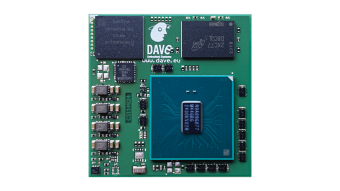
SoM/SBC
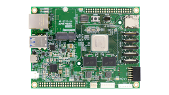
RZ/T2H ZERO System on Module (SoM)
The ZERO SOM, developed by DAVE Embedded Systems, is a system on module (SoM) featuring the Renesas RZ/T2H application processor. This SOM is part of the Harsh Line portfolio from DAVE Embedded Systems, which ensures maximum performance and integration. With a minimum availability of 15 years, it meets the needs of reliable and durable industrial applications. ZERO SOM includes up to 3 industrial MAC Ethernet ports, up to 9 motor control axes, and a safety management system, making it ideal for industrial, safe, and secure connected applications.
Provided By:
DAVE Embedded Systems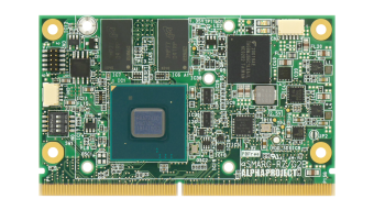
SoM/SBC
SMARC RZ/G2E System on Module (SoM)
Provides a System on Module (SoM) based on the Renesas RZ/G2E. Delivers dual Arm® Cortex®-A53 processing with an integrated PowerVR GE8300 3D graphics engine and supports Full HD video encoding and decoding. Supports high-speed interfaces such as PCI Express and display connectivity, making it suitable for HMI applications. Complies with the SMARC 2.1 standard form factor to enable flexible and scalable system design with high compatibility and expandability.
Provided By:
AlphaProject Co.,Ltd.