
| CAD 模型: | View CAD Model |
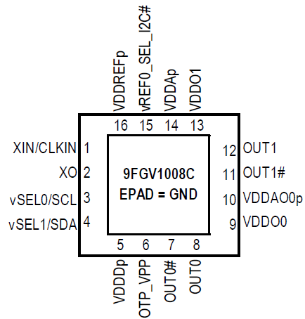
| Pkg. Type: | LGA |
| Pkg. Code: | LTG16 |
| Lead Count (#): | 16 |
| Pkg. Dimensions (mm): | 3.0 x 3.0 x 1.1 |
| Pitch (mm): | 0.5 |
| Moisture Sensitivity Level (MSL) | 3 |
| Pb (Lead) Free | Yes |
| ECCN (US) | EAR99 |
| HTS (US) | 8542.39.0090 |
| Lead Count (#) | 16 |
| Carrier Type | Reel |
| Moisture Sensitivity Level (MSL) | 3 |
| Advanced Features | Reference Output, Spread Spectrum, Programmable Clock |
| Core Voltage (V) | 1.8V, 2.5V, 3.3V |
| Input Freq (MHz) | 1 - 240 |
| Outputs (#) | 3 |
| Output Banks (#) | 3 |
| Output Freq Range (MHz) | 10 - 325 |
| Output Impedance | 85, 100 |
| Output Type | LP-HCSL, LVCMOS, LVDS |
| Output Voltage (V) | 1.8V, 2.5V, 3.3V |
| Prog. Clock | No |
| Qty. per Reel (#) | 3000 |
| Supply Voltage (V) | 1.8 - 1.8, 2.5 - 2.5, 3.3 - 3.3 |
| Qty. per Carrier (#) | 0 |
| Xtal Freq (MHz) | 8 - 50 |
| Pb (Lead) Free | Yes |
| Pb Free Category | e4 Au |
| Temp. Range (°C) | -40 to 85°C |
| Accepts Spread Spec Input | Yes |
| App Jitter Compliance | PCIe Gen1, PCIe Gen2, PCIe Gen3, PCIe Gen4 |
| Architecture | Common, SRNS, SRIS |
| C-C Jitter Max P-P (ps) | 50 |
| Diff. Output Signaling | LP-HCSL, LVDS |
| Diff. Outputs | 2 |
| Family Name | PhiClock |
| Function | Generator |
| Input Type | Crystal, LVCMOS |
| Inputs (#) | 1 |
| Length (mm) | 3 |
| MOQ | 3000 |
| Package Area (mm²) | 25 |
| Phase Jitter Typ RMS (ps) | 0.224 |
| Pitch (mm) | 0.5 |
| Pkg. Dimensions (mm) | 3.0 x 3.0 x 1.1 |
| Pkg. Type | LGA |
| Power Consumption Typ (mW) | 100 |
| Product Category | PhiClock, PCI Express Clocks, Programmable Clocks |
| Prog. Interface | I2C, OTP |
| Reel Size (in) | 13 |
| Reference Output | No |
| Spread Spectrum | Yes |
| Tape & Reel | Yes |
| Thickness (mm) | 1.1 |
| Width (mm) | 3 |
| Xtal Inputs (#) | 1 |
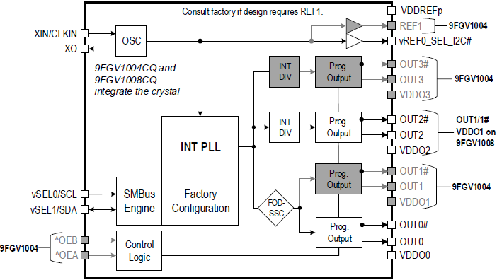
The 9FGV1008 is a member of Renesas' PhiClock™ programmable clock generator family. The 9FGV1008 provides one integer frequency, one copy of a fractional or spread spectrum output frequency, and one copy of the crystal reference input. Two select pins allow for hardware selection of the desired configuration, or two I2C bits allow easy software selection of the desired configuration. The user may configure any one of the four OTP configurations as the default when operating in I2C mode. Four unique I2C addresses are available, allowing easy I2C access to multiple components.