特性
- LP-HCSL outputs with 85Ω Zout; eliminates 76 termination resistors, saves 130mm² area
- PCIe Gen 1–5 compliance
- 8 OE# pins configurable to control up to 16 outputs; easy power management
- 9 selectable SMBus addresses; multiple devices can share same SMBus segment
- Selectable PLL BW; minimizes jitter peaking in cascaded PLL topologies
- Hardware/SMBus control of PLL bandwidth and bypass; change mode without power cycle
- Spread spectrum compatible; tracks spreading input clock for EMI reduction
- 100MHz PLL mode; UPI support
- DIF input and DIF outputs on outer row of pins; easy board routing
- 6 x 6 mm dual-row 80-GQFN; smallest 19-output Z-buffer


9ZXL15x0D-19xxD - Block Diagram
描述
The 9ZXL1951D is a second-generation, enhanced performance DB1900ZL derivative buffer. The part is a pin-compatible upgrade to the 9ZXL1951A, offering a much improved phase jitter performance. It has 8 OE# pins that can be configured via SMBus to control up to 16 of the device's 19 outputs, and is packaged in a 6 x 6 mm QFN package for maximum space savings. A fixed external feedback maintains low drift for critical QPI/UPI applications.
产品参数
| 属性 | 值 |
|---|---|
| Diff. Outputs | 19 |
| Diff. Output Signaling | LP-HCSL |
| Output Freq Range (MHz) | 1 - 400 |
| Diff. Inputs | 1 |
| Diff. Input Signaling | HCSL |
| Accepts Spread Spec Input | Yes |
| Power Consumption Typ (mW) | 712 |
| Supply Voltage (V) | 3.3 - 3.3 |
| Output Type | LP-HCSL |
| Diff. Termination Resistors | 0 |
| Package Area (mm²) | 100 |
| Battery Backup | No |
| Battery Seal | No |
| CPU Supervisory Function POR | No |
| Crystal Frequency Trimming | No |
| Frequency Out Pin | No |
| Inputs (#) | 1 |
| Input Freq (MHz) | 33 - 150 |
| Function | Zero Delay Buffer |
| Input Type | HCSL |
| Output Banks (#) | 1 |
| Core Voltage (V) | 3.3 |
| Output Voltage (V) | 0.7 |
| Product Category | PCI Express Clocks, Processor Clock Buffers, Zero Delay Buffers |
封装选项
| Pkg. Type | Pkg. Dimensions (mm) | Lead Count (#) | Pitch (mm) |
|---|---|---|---|
| VFQFPN | 6.0 x 6.0 x 0.85 | 80 | 0.5 |
Renesas Boards & Kits
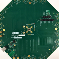
EVK9ZXL1951D
有效
Evaluation Kit for 19-Output DB1900Z for PCIe Gen1-4 and QPI/UPI
The evaluation board is designed to help the customer evaluate the 9ZXL1951D. The device is programmable through an SMBus interface. The user guide details the board set and connection, as well as the companion Graphical User Interface (GUI) installation for communicating with the device. The... 阅读详情
