封装信息
| CAD 模型: | View CAD Model |
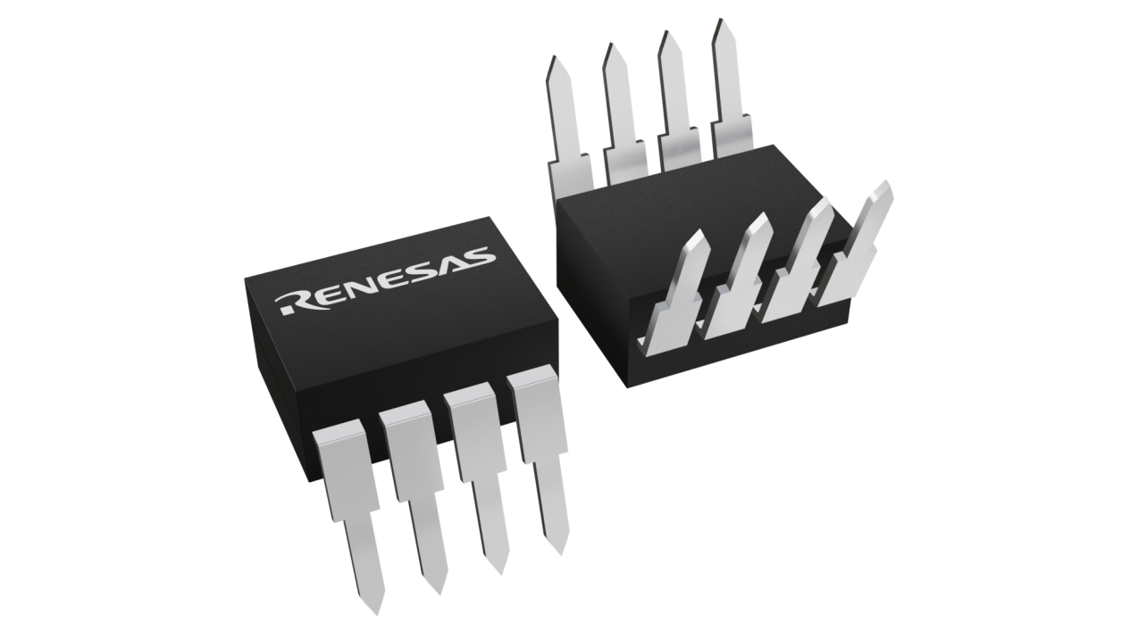
| Pkg. Type: | PDIP |
| Pkg. Code: | EWD |
| Lead Count (#): | 8 |
| Pkg. Dimensions (mm): | 9.7 x 6.6 x 3.94 |
| Pitch (mm): | 2.5 |
环境和出口类别
| Moisture Sensitivity Level (MSL) | Not Applicable |
| Pb (Lead) Free | Yes |
| ECCN (US) | EAR99 |
| HTS (US) | 8542.33.0001 |
| RoHS (CA3140AEZ) | 下载 |
产品属性
| Lead Count (#) | 8 |
| Carrier Type | Tube |
| Moisture Sensitivity Level (MSL) | Not Applicable |
| Pitch (mm) | 2.5 |
| Pkg. Dimensions (mm) | 9.7 x 6.6 x 3.94 |
| Pb (Lead) Free | Yes |
| Pb Free Category | Pb-Free 100% Matte Tin Plate w/Anneal-e3 |
| MOQ | 3000 |
| Temp. Range (°C) | -55 to +125°C |
| Country of Assembly | MALAYSIA, TAIWAN, PHILIPPINES |
| Country of Wafer Fabrication | USA |
| AVOL (dB) | 100 |
| Bandwidth (MHz) | 4.5 |
| CMRR (dB) | 90 |
| Channels (#) | 1 |
| Die Sale Availability? | No |
| Enable | Strobe |
| Flow | Harsh Environment & MIL-STD-883 |
| Gain Min | 1 |
| IBIAS (nA) | 0.01 |
| IOUT (mA) | 40 |
| IS per Amp (mA) | 4 |
| Length (mm) | 9.7 |
| Noise VN (nV/√Hz) | 12 |
| Offset Voltage (Max) (mV) | 2 |
| Offset Voltage (max) | 2mV |
| Output Headroom (V) | 2 |
| PROTO Availability? | No |
| PSRR (db) | 80 |
| Pkg. Type | PDIP |
| Price (USD) | $1.67128 |
| Qualification Level | Standard |
| Rail-to-Rail Input | -Vs |
| Rail-to-Rail Input/Output | No |
| Rail-to-Rail Output | No |
| Rating | Harsh Environment |
| Single Supply Voltage Range (V) | 4 - 36 |
| Slew Rate (V/µs) | 9 |
| Supply Voltage (max) (V) | 36 - 36 |
| Supply Voltage (min) (V) | 4 - 4 |
| Thermal Shutdown | No |
| Thickness (mm) | 3.94 |
| Topology [Rail 1] | VFA |
| VOUT (V) | 27.4 |
| VS (Max) (V) | 36 |
| VS (Min) (V) | 4 |
| Width (mm) | 6.6 |
| field__slew_rate_typical_ | 9 |
有关 CA3140A 的资源
描述
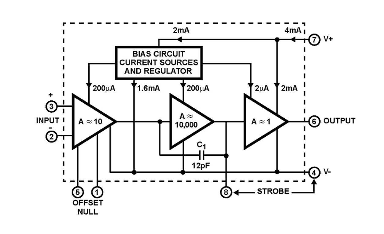
The CA3140A and CA3140 are integrated circuit operational amplifiers that combine the advantages of high voltage PMOS transistors with high voltage bipolar transistors on a single monolithic chip. The CA3140A and CA3140 BiMOS operational amplifiers feature gate protected MOSFET (PMOS) transistors in the input circuit to provide very high input impedance, very low input current, and High-Speed performance. The CA3140A and CA3140 operate at supply voltage from 4V to 36V (either single or dual supply). These operational amplifiers are internally phase compensated to achieve stable operation in unity gain follower operation, and additionally, have access terminal for a supplementary external capacitor if additional frequency roll-off is desired. Terminals are also provided for use in applications requiring input offset voltage nulling. The use of PMOS field effect transistors in the input stage results in common mode input voltage capability down to 0. 5V below the negative supply terminal, an important attribute for single supply applications. The output stage uses bipolar transistors and includes built-in protection against damage from load terminal short circuiting to either supply rail or to ground. FN957 The CA3140A and CA3140 are intended for operation at supply voltages up to 36V (±18V).

