封装信息
| CAD 模型: | View CAD Model |
| Pkg. Type: | CFP |
| Pkg. Code: | KBG |
| Lead Count (#): | 16 |
| Pkg. Dimensions (mm): | 10.4 x 6.9 x 0.00 |
| Pitch (mm): | 1.3 |
环境和出口类别
| Moisture Sensitivity Level (MSL) | Not Applicable |
| Pb (Lead) Free | Exempt |
| ECCN (US) | |
| HTS (US) |
产品属性
| Pkg. Type | CFP |
| Lead Count (#) | 16 |
| Carrier Type | Tray |
| Moisture Sensitivity Level (MSL) | Not Applicable |
| Pitch (mm) | 1.3 |
| Pkg. Dimensions (mm) | 10.4 x 6.9 x 0.00 |
| DLA SMD | 5962R9661501VXC |
| Pb (Lead) Free | Exempt |
| Pb Free Category | Gold Plate over compliant Undercoat-e4 |
| MOQ | 25 |
| Temp. Range (°C) | -55 to +125°C |
| DSEE (MeV·cm2/mg) | 75 |
| Length (mm) | 10.4 |
| Qualification Level | QML Class V (space) |
| Rating | Space |
| TID HDR (krad(Si)) | 100 |
| TID LDR (krad(Si)) | ELDRS free |
| Width (mm) | 6.9 |
有关 CD4099BMS 的资源
描述
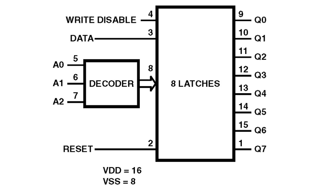
The CD4099BMS 8-bit addressable latch is a serial input, parallel output storage register that can perform a variety of functions. Data are inputted to a particular bit in the latch when that bit is addressed (by means of inputs A0, A1, A2) and when WRITE DISABLE is at a low level. When WRITE DISABLE is high, data entry is inhibited; however, all 8 outputs can be continuously read independent of WRITE DISABLE and address inputs. A master RESET input is available, which resets all bits to a logic 0 level when RESET and WRITE DISABLE are at a high level. When RESET is at a high level, and WRITE DISABLE is at a low level, the latch acts as a 1 of 8 demultiplexer; the bit that is addressed has an active output that follows the data input, while all unaddressed bits are held to a logic 0 level. The CD4099BMS is supplied in these 16-lead outline packages: Braze Seal DIP H4X, Frit Seal DIP H1F, Ceramic Flatpack H6W.
