特性
- High Voltage Type (20V Rating)
- Independence of Power Supply Sequence Considerations VCC can Exceed VDD Input Signals can Exceed Both VCC and VDD
- Up and Down Level Shifting Capability
- Shiftable Input Threshold for Either CMOS or TTL Compatibility
- 100% Tested for Quiescent Current at 20V
- 5V, 10V and 15V Parametric Ratings
- Standardized Symmetrical Output Characteristics
- Maximum Input Current of 1µA at 18V Over Full Package Temperature Range; 100nA at 18V and +25°C
- Meets All Requirements of JEDEC Tentative Standard No. 13B, "Standard Specifications for Description of 'B' Series CMOS Devices"
描述
Support is limited to customers who have already adopted these products.
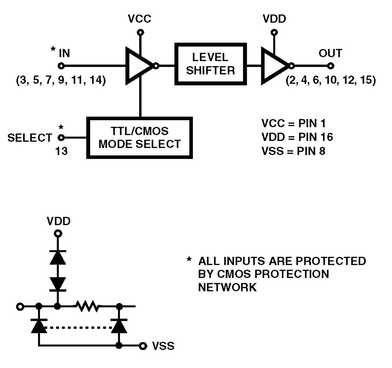
CD4504BMS hex voltage level shifter consists of six circuits which shift input signals from the VCC logic level to the VDD logic level. To shift TTL signals to CMOS logic levels, the SELECT input is at the VCC HIGH logic state. When the SELECT input is at a LOW logic state, each circuit translates signals from one CMOS level to another. The CD4504BMS is supplied in these 16-lead outline packages: Frit Seal DIP H1F Ceramic Flatpack H6W
当前筛选条件

