封装信息
| CAD 模型: | View CAD Model |
| Pkg. Type: | DFN |
| Pkg. Code: | LBB |
| Lead Count (#): | 10 |
| Pkg. Dimensions (mm): | 3.00 x 3.00 x 0.90 |
| Pitch (mm): | 0.5 |
环境和出口类别
| Moisture Sensitivity Level (MSL) | 3 |
| Pb (Lead) Free | Yes |
| ECCN (US) | EAR99 |
| HTS (US) | 8542.39.0090 |
| RoHS (ISL80112IRAJZ-T) | 下载 |
产品属性
| Lead Count (#) | 10 |
| Carrier Type | Reel |
| Moisture Sensitivity Level (MSL) | 3 |
| Pb (Lead) Free | Yes |
| Pb Free Category | Pb-Free 100% Matte Tin Plate w/Anneal-e3 |
| Temp. Range (°C) | -40 to +85°C |
| Country of Assembly | MALAYSIA |
| Country of Wafer Fabrication | TAIWAN |
| Drop Out Voltage (Typical) | 53 @ 2A |
| Enable/Shutdown | Yes |
| External Bias | Yes |
| Fixed Output Voltage Option | No |
| Input Voltage (Max) (V) | 3.6 |
| Input Voltage (Min) (V) | 0.7 |
| Input Voltage Range (V) | 1 - 3.6 |
| Length (mm) | 3 |
| MOQ | 6000 |
| Noise (10Hz to 100kHz) (μVrms) | 100 |
| O/P Voltage Accuracy (±%) | 1.6 |
| Output Current 1 (Max) (A) | 2 |
| Output Voltage (Max) (V) | 3.3 |
| Output Voltage (Min) (V) | 0.5 |
| Output Voltage Range (V) | 0.8 - 3.3 |
| PGOOD Output | Yes |
| PORs (#) | 1 |
| PSRR (db) | 80 |
| Parametric Category | Linear Regulators (LDO) |
| Pitch (mm) | 0.5 |
| Pkg. Dimensions (mm) | 3.0 x 3.0 x 0.90 |
| Pkg. Type | DFN |
| Price (USD) | $1.47827 |
| Qualification Level | Standard |
| Quiescent Current | 3500 µA |
| Thickness (mm) | 0.9 |
| Width (mm) | 3 |
有关 ISL80112 的资源
描述
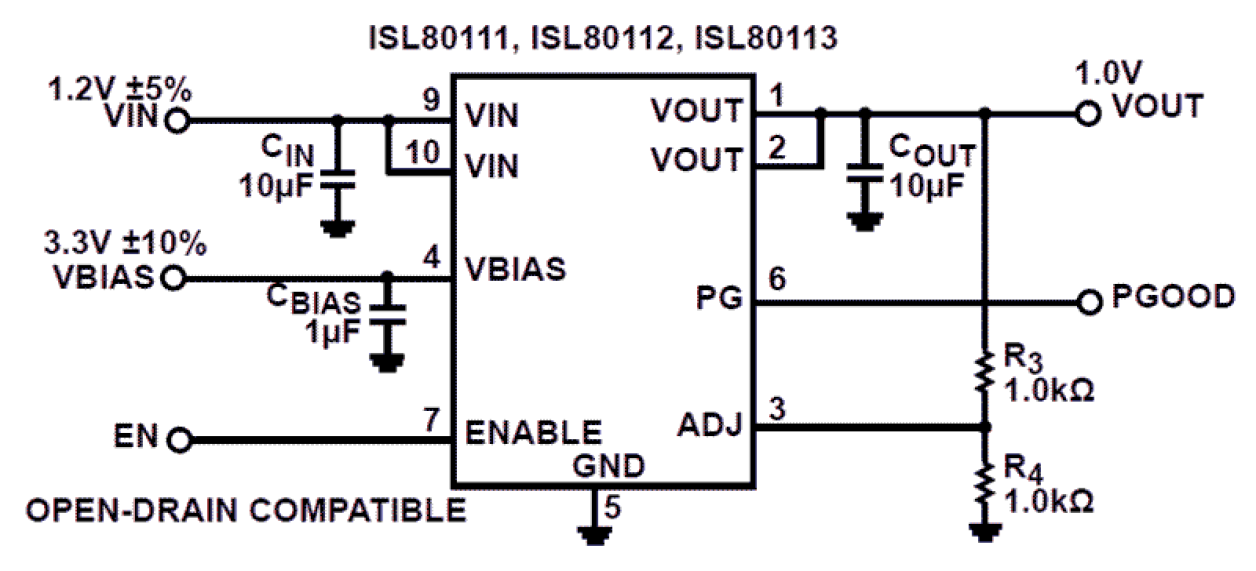
The ISL80111, ISL80112, and ISL80113 are ultra low dropout LDOs providing the optimum balance between performance, size and power consumption in size constrained designs for data communication, computing, storage and medical applications. These LDOs are specified for 1A, 2A and 3A of output current and are optimized for low voltage conversions. Operating with a VIN of 1V to 3. 6V and with a legacy 2. 9V to 5. 5V on the BIAS, the VOUT is adjustable from 0. 8V to 3. 3V. With a VIN PSRR greater than 40dB at 100kHz makes these LDOs an ideal choice in noise sensitive applications. The guaranteed ±1. 6% VOUT accuracy overall conditions lend these parts to supplying an accurate voltage to the latest low voltage digital ICs. An enable input allows the part to be placed into a low quiescent current shutdown mode. A submicron CMOS process is utilized for this product family to deliver best-in-class analog performance and overall value for applications in need of input voltage conversions typically below 2. 5V. It also has the superior load transient regulation unique to a NMOS power stage. These LDOs consume significantly lower quiescent current as a function of load compared to bipolar LDOs.
