特性
- Dual output, 6A peak currents, can be paralleled
- Dual AND-ed input logic, (input and enable)
- Typical ON-resistance <1Ω
- Specified Miller plateau drive currents
- Very low thermal impedance (θJC = 3°C/W)
- Hysteretic Input logic levels for 3.3V CMOS, 5V CMOS, TTL, and Logic levels proportional to VDD
- Precision threshold inputs for time delays with external RC components
- 20ns rise and fall time driving a 10nF load.
描述
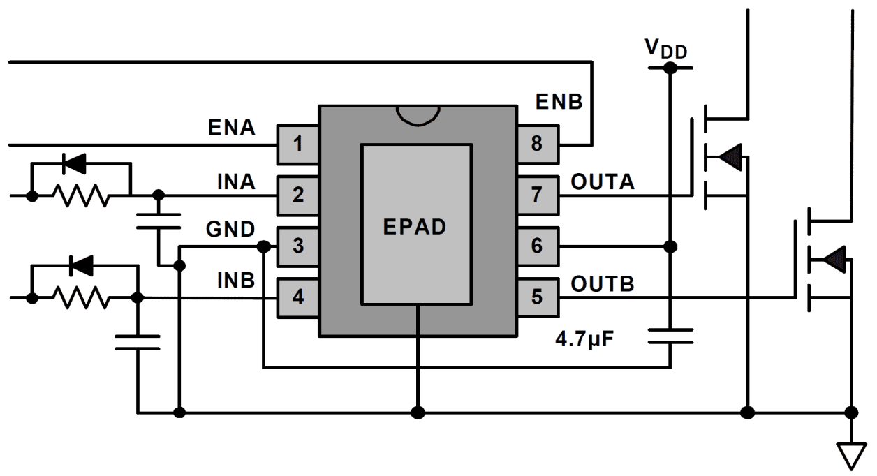
The ISL89163, ISL89164, and ISL89165 are high-speed, 6A, dual channel MOSFET drivers with enable inputs. Precision thresholds on all logic inputs allow the use of external RC circuits to generate accurate and stable time delays on both the main channel inputs, INA and INB, and the enable inputs, ENA and ENB. The precision delays capable of these precise logic thresholds makes these parts very useful for dead-time control and synchronous rectifiers. Note that the enable and input logic inputs can be interchanged for alternate logic implementations. Three input logic thresholds are available: 3. 3V (CMOS), 5. 0V (CMOS or TTL compatible), and CMOS thresholds that are proportional to VDD. At high switching frequencies, these MOSFET drivers use very little internal bias currents. Separate, non-overlapping drive circuits are used to drive each CMOS output FET to prevent shoot-through currents in the output stage. The start-up sequence is designed to prevent unexpected glitches when VDD is being turned on or turned off. When VDD ~1V, an internal 10kΩ resistor between the output and ground helps to keep the output voltage low. When ~1V VDD UV, both outputs are driven low with very low resistance and the logic inputs are ignored. This insures that the driven FETs are off. When VDD > UVLO, and after a short delay, the outputs now respond to the logic inputs.
产品参数
| 属性 | 值 |
|---|---|
| Drivers (#) | 2 |
| Input Voltage (Max) (V) | 16 |
| Peak Output Current IPK (A) | 6 |
| Rise Time (μs) | 20 |
| Fall Time | 0.02 |
| Turn On Delay (ns) | 25 |
| Turn Off Delay (ns) | 25 |
| IS (mA) | 5 |
| Input Supply Range (V) | 4.5 - 16 |
| Output Signal Range | 0 to +16 |
| Input Signal Range | 0 to 16 |
封装选项
| Pkg. Type | Pkg. Dimensions (mm) | Lead Count (#) | Pitch (mm) |
|---|---|---|---|
| TDFN | 3.0 x 3.0 x 0.75 | 8 | 0.5 |
应用方框图
 | 高效数字电源 全新的 CrM PFC + LLC 电源,提供高效率和精确的电源管理。 |
 | 并网太阳能微型逆变器 太阳能微型逆变器系统,带有高性能MCU、MOSFET和驱动器的并网单元。 |
 | 便携式 EV 充电器 便携式直流充电器,适用于由 48V 电池组供电的电动汽车,具有蓝牙连接功能。 |
 | 高功率 AC/DC 电源适配器 这款 AC/DC 电源适配器充电器具有 PFC 稳定性、ZVS 控制器和易于配置。 |
 | 5G 基础设施电源 5G 电源为各种 5G 应用提供高效率、低噪声和强大的性能。 |
 | 带无线控制的 PC 水冷系统 先进的 PC 水冷器,具有无线控制、散热高效和配置灵活等特点。 |
 | 智能太阳能灌溉泵控制器 太阳能灌溉系统提高了能源效率,减少了对电网的依赖,并实现了智能精确控制。 |
其他应用
- Synchronous Rectifier (SR) Driver
- Switch mode power supplies
- Motor Drives, Class D amplifiers, UPS, Inverters
- Pulse Transformer driver
- Clock/Line driver
当前筛选条件

