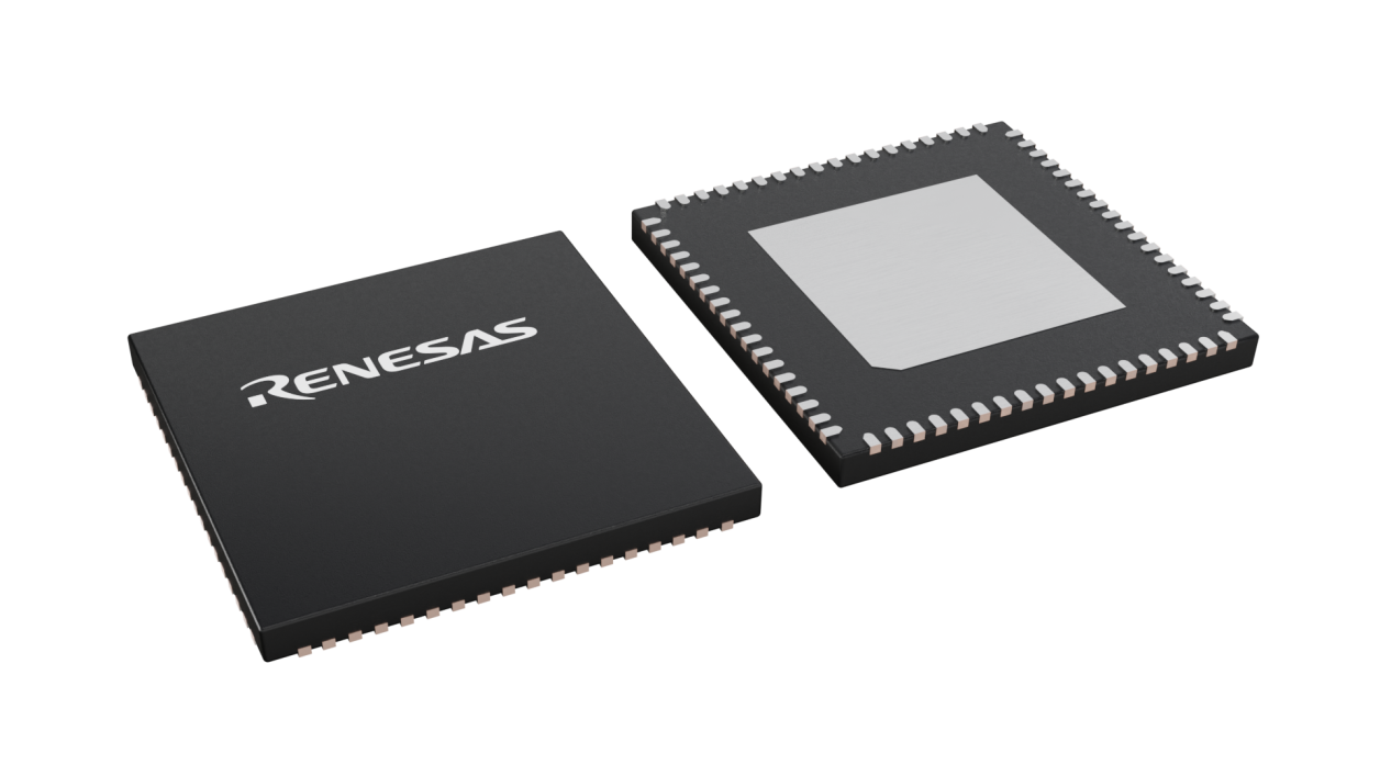
封装信息
| CAD 模型: | View CAD Model |
| Pkg. Type: | QFN |
| Pkg. Code: | LSL |
| Lead Count (#): | 72 |
| Pkg. Dimensions (mm): | 10.0 x 10.0 x 0.90 |
| Pitch (mm): | 0.5 |
环境和出口类别
| Moisture Sensitivity Level (MSL) | 3 |
| Pb (Lead) Free | Yes |
| ECCN (US) | 3A991.c.2 |
| HTS (US) | 8542.39.0030 |
| RoHS (KAD5612P-12Q72) | 下载 |
产品属性
| Lead Count (#) | 72 |
| Carrier Type | Tray |
| Moisture Sensitivity Level (MSL) | 3 |
| Pb (Lead) Free | Yes |
| Pb Free Category | Nickel/Palladium/Gold-e4 |
| Temp. Range (°C) | -40 to +85°C |
| Country of Assembly | MALAYSIA, CANADA |
| Country of Wafer Fabrication | TAIWAN |
| Channels (#) | 2 |
| Conversion Rate (Max) (kSPS) | 125000 |
| Differential NonLinearity LSB | 0.8 |
| Digital Supply Voltage (V) | 1.8 - 1.8 |
| Input BW (MHz) | 1300 |
| Input VIN ((VPP, differential)) | 1.47 |
| Integral NonLinearity LSB | 2.5 |
| Interface | LVDS/LVCMOS |
| Length (mm) | 10 |
| MOQ | 56 |
| Pitch (mm) | 0.5 |
| Pkg. Dimensions (mm) | 10.0 x 10.0 x 0.90 |
| Pkg. Type | QFN |
| Power Consumption (mW) | 342 |
| Price (USD) | $68.57304 |
| Qualification Level | Standard |
| Resolution (bits) | 12 |
| SFDR (dB) (dB) | 80.4 |
| SNR (dbFS) | 67.2 |
| Supply Voltage (V) | 1.8 - 1.8 |
| Thickness (mm) | 0.9 |
| Width (mm) | 10 |
有关 KAD5612P-12 的资源
描述
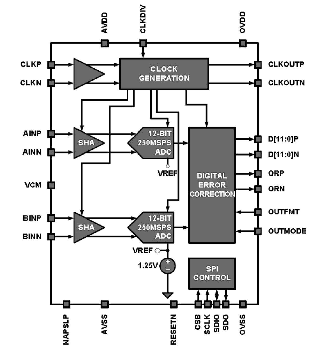
The KAD5612P is a family of low-power, high-performance, dual-channel 12-bit, analog-to-digital converters. Designed with FemtoCharge™ technology on a standard CMOS process, the family supports sampling rates of up to 250MSPS. The KAD5612P-25 is the fastest member of this pin-compatible family, which also features sample rates of 210MSPS (KAD5612P-21), 170MSPS (KAD5612P-17) and 125MSPS (KAD5612P-12). A Serial Peripheral Interface (SPI) port allows for extensive configurability, as well as fine control of gain, skew and offset matching between the two converter cores. Digital output data is presented in selectable LVDS or CMOS formats. The KAD5612P is available in a 72 Ld QFN package with an exposed paddle. Performance is specified over the full industrial temperature range (-40°C to +85°C).

