特性
- Jitter below 100fs RMS maximum (10kHz to 20MHz)
- PLL core consists of fractional-feedback Analog PLL (APLL)
- APLL frequency independent of input / crystal frequency
- Operates as a frequency synthesizer or Digitally Controlled Oscillator (DCO)
- DCO has tuning granularity of < 1ppb
- Programmable status output
- 4 differential / 8 LVCMOS outputs
- Any frequency from 10MHz to 1GHz (180MHz for LVCMOS)
- Programmable output buffer supports HCSL (DC-coupled), LVDS/LVPECL/CML (AC-coupled) or two LVCMOS
- Differential output swing is selectable: 400mV to 800mV
- Output clock phase individually adjustable in 100ps steps
- Output Enable input with programmable effect
- Supports up to 1MHz I2C or up to 20MHz SPI serial processor port
- Can configure itself automatically after reset via internal customer-definable One-Time Programmable (OTP) memory with up to four different configurations
- 4 × 4 mm 28-VFQFPN package
描述
The RC22514A is a small, low-power timing component designed to be placed immediately adjacent to a PHY, switch, ASIC or FPGA that requires several reference clocks with jitter performance less than 100fs (max). The RC22514A can act as a frequency synthesizer to locally generate the reference clock or as a DCO for frequency margining or OTN clock applications, relying on an internal crystal reference source.
试用自定义部件配置工具。
产品参数
| 属性 | 值 |
|---|---|
| Diff. Outputs | 4 |
| Outputs (#) | 4 |
| Output Type | LVCMOS, HCSL, LVDS |
| Output Freq Range (MHz) | 10 - 1000 |
| Inputs (#) | 0 |
| Output Banks (#) | 4 |
| Core Voltage (V) | 1.8V, 3.3V |
| Output Voltage (V) | 1.8 |
| Feedback Input | No |
| Product Category | FemtoClock 2, Ultra-Low Jitter Clocks (<300 fs RMS), Extreme Performance Clocks (<150 fs RMS), Network Synchronization, PDH and SONET/SDH Clocks, Programmable Clocks |
封装选项
| Pkg. Type | Pkg. Dimensions (mm) | Lead Count (#) | Pitch (mm) |
|---|---|---|---|
| VFQFPN | 4.0 x 4.0 x 1.5 | 28 | 0.4 |
试用自定义部件配置工具。
| Part Number | Status | Samples | Longevity | Stock | Package | Budgetary Price (USD) | Lead Count (#) | Carrier Type | Moisture Sensitivity Level (MSL) | Qty. per Reel (#) | Qty. per Carrier (#) | Pb (Lead) Free | Pb Free Category | Temp. Range (°C) | Country of Assembly | Country of Wafer Fabrication |
|---|---|---|---|---|---|---|---|---|---|---|---|---|---|---|---|---|
| RC22514A000GNL#BB0 | Active | Available | 2040 Apr | In Stock | VFQFPN | 1ku | $7.04 | 28# | Tray | 3 | 0 | 490# | Yes | e3 Sn | -40 to 85°C | MALAYSIA | SINGAPORE |
| RC22514A000GNL#KB0 | Active | N/A | 2040 Apr | Out of Stock | VFQFPN | 1ku | $7.04 | 28# | Reel | 3 | 2500# | 0 | Yes | e3 Sn | -40 to 85°C | MALAYSIA | SINGAPORE |
- 手册 - 软件英语PDF 2.21 MB R31US0012EU0102 Rev.1.02 2024年5月23日
- 应用说明英语PDF 129 KB 2021年8月04日AI 生成的摘要: FemtoClock 2 enables precise frequency margining through I2C-controlled configuration of output clock frequencies. It uses a fractional-N APLL with a 27-bit feedback divider for fine frequency resolution and integer output dividers for individual outputs. Frequency changes can be made glitch-free by adjusting output dividers or more precisely by modifying the fractional feedback divider, which may require APLL recalibration if changes exceed ±0.1%. The document details register addressing, frequency adjustment methods, and calibration procedures to optimize clock output performance.
- 应用说明英语PDF 256 KB 2021年7月05日AI 生成的摘要: The document explains methods to generate a 1.2V LVCMOS signal from a 1.8V LVCMOS output by attenuating the amplitude without lowering the driver voltage. It details typical LVCMOS driver and receiver configurations, impedance matching using source termination, and the use of a parallel resistor at the receiver input to reduce signal amplitude. Simulation and measurement results demonstrate that adding a parallel resistor effectively lowers the voltage to 1.2V while maintaining signal integrity and minimal impact on jitter and frequency. This approach supports flexible amplitude adjustment for various low-voltage LVCMOS requirements in clock signal applications.
- 应用说明英语PDF 495 KB 7WDXRDKU4E7E-5-57312 2014年5月12日
- 应用说明英语PDF 120 KB 7WDXRDKU4E7E-5-57289 2014年5月06日
推荐文档 (1)
数据手册 (1)
- 手册 - 软件英语PDF 2.21 MB R31US0012EU0102 Rev.1.02 2024年5月23日
手册和指南 (3)
- 应用说明英语PDF 129 KB 2021年8月04日AI 生成的摘要: FemtoClock 2 enables precise frequency margining through I2C-controlled configuration of output clock frequencies. It uses a fractional-N APLL with a 27-bit feedback divider for fine frequency resolution and integer output dividers for individual outputs. Frequency changes can be made glitch-free by adjusting output dividers or more precisely by modifying the fractional feedback divider, which may require APLL recalibration if changes exceed ±0.1%. The document details register addressing, frequency adjustment methods, and calibration procedures to optimize clock output performance.
- 应用说明英语PDF 256 KB 2021年7月05日AI 生成的摘要: The document explains methods to generate a 1.2V LVCMOS signal from a 1.8V LVCMOS output by attenuating the amplitude without lowering the driver voltage. It details typical LVCMOS driver and receiver configurations, impedance matching using source termination, and the use of a parallel resistor at the receiver input to reduce signal amplitude. Simulation and measurement results demonstrate that adding a parallel resistor effectively lowers the voltage to 1.2V while maintaining signal integrity and minimal impact on jitter and frequency. This approach supports flexible amplitude adjustment for various low-voltage LVCMOS requirements in clock signal applications.
应用说明和白皮书 (20)
No Results Found.
确保所有关键词拼写正确。
尝试使用更少、不同或更宽泛的词语来改变搜索结果。
如果您使用了筛选器,请考虑取消选择某些筛选器选项以扩大搜索结果。
- 搜索我们丰富的知识库,帮助您解答常见问题
- 前往支持论坛,获取瑞萨电子技术专家和社群的帮助
No Results Found.
确保所有关键词拼写正确。
尝试使用更少、不同或更宽泛的词语来改变搜索结果。
如果您使用了筛选器,请考虑取消选择某些筛选器选项以扩大搜索结果。
- 搜索我们丰富的知识库,帮助您解答常见问题
- 前往支持论坛,获取瑞萨电子技术专家和社群的帮助
No Results Found.
确保所有关键词拼写正确。
尝试使用更少、不同或更宽泛的词语来改变搜索结果。
如果您使用了筛选器,请考虑取消选择某些筛选器选项以扩大搜索结果。
- 搜索我们丰富的知识库,帮助您解答常见问题
- 前往支持论坛,获取瑞萨电子技术专家和社群的帮助
No Results Found.
确保所有关键词拼写正确。
尝试使用更少、不同或更宽泛的词语来改变搜索结果。
如果您使用了筛选器,请考虑取消选择某些筛选器选项以扩大搜索结果。
- 搜索我们丰富的知识库,帮助您解答常见问题
- 前往支持论坛,获取瑞萨电子技术专家和社群的帮助
No Results Found.
确保所有关键词拼写正确。
尝试使用更少、不同或更宽泛的词语来改变搜索结果。
如果您使用了筛选器,请考虑取消选择某些筛选器选项以扩大搜索结果。
- 搜索我们丰富的知识库,帮助您解答常见问题
- 前往支持论坛,获取瑞萨电子技术专家和社群的帮助
No Results Found.
确保所有关键词拼写正确。
尝试使用更少、不同或更宽泛的词语来改变搜索结果。
如果您使用了筛选器,请考虑取消选择某些筛选器选项以扩大搜索结果。
- 搜索我们丰富的知识库,帮助您解答常见问题
- 前往支持论坛,获取瑞萨电子技术专家和社群的帮助
No Results Found.
确保所有关键词拼写正确。
尝试使用更少、不同或更宽泛的词语来改变搜索结果。
如果您使用了筛选器,请考虑取消选择某些筛选器选项以扩大搜索结果。
- 搜索我们丰富的知识库,帮助您解答常见问题
- 前往支持论坛,获取瑞萨电子技术专家和社群的帮助
No Results Found.
确保所有关键词拼写正确。
尝试使用更少、不同或更宽泛的词语来改变搜索结果。
如果您使用了筛选器,请考虑取消选择某些筛选器选项以扩大搜索结果。
- 搜索我们丰富的知识库,帮助您解答常见问题
- 前往支持论坛,获取瑞萨电子技术专家和社群的帮助
No Results Found.
确保所有关键词拼写正确。
尝试使用更少、不同或更宽泛的词语来改变搜索结果。
如果您使用了筛选器,请考虑取消选择某些筛选器选项以扩大搜索结果。
- 搜索我们丰富的知识库,帮助您解答常见问题
- 前往支持论坛,获取瑞萨电子技术专家和社群的帮助
No Results Found.
确保所有关键词拼写正确。
尝试使用更少、不同或更宽泛的词语来改变搜索结果。
如果您使用了筛选器,请考虑取消选择某些筛选器选项以扩大搜索结果。
- 搜索我们丰富的知识库,帮助您解答常见问题
- 前往支持论坛,获取瑞萨电子技术专家和社群的帮助
Renesas Boards & Kits
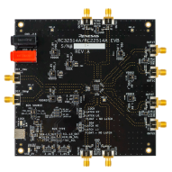
FemtoClock™ 2 Evaluation Kit
This is the evaluation kit for the RC32514A and RC22514A. The board will come populated with an RC32514. The RC22514 is functionally a subset of the RC32514A, so this board can be used to evaluate either or both of the devices. Refer to the device's web pages for additional details on the... 阅读详情
筛选
当前筛选条件
软件与工具
按类型筛选
按供应商筛选
样例程序
按应用筛选
按功能筛选
按编译器筛选
按 IDE 筛选
模拟模型
Partner Solutions
No Results Found.
确保所有关键词拼写正确。
尝试使用更少、不同或更宽泛的词语来改变搜索结果。
如果您使用了筛选器,请考虑取消选择某些筛选器选项以扩大搜索结果。
- 搜索我们丰富的知识库,帮助您解答常见问题
- 前往支持论坛,获取瑞萨电子技术专家和社群的帮助
软件与工具 (1)
No Results Found.
确保所有关键词拼写正确。
尝试使用更少、不同或更宽泛的词语来改变搜索结果。
如果您使用了筛选器,请考虑取消选择某些筛选器选项以扩大搜索结果。
- 搜索我们丰富的知识库,帮助您解答常见问题
- 前往支持论坛,获取瑞萨电子技术专家和社群的帮助
模拟模型 (1)
No Results Found.
确保所有关键词拼写正确。
尝试使用更少、不同或更宽泛的词语来改变搜索结果。
如果您使用了筛选器,请考虑取消选择某些筛选器选项以扩大搜索结果。
- 搜索我们丰富的知识库,帮助您解答常见问题
- 前往支持论坛,获取瑞萨电子技术专家和社群的帮助
Demonstration of Renesas’ Lab on the Cloud virtual environment for FemtoClock®2 ultra-low phase noise synthesizer and jitter attenuator.
An introduction to Renesas’ FemtoClock®2 jitter cleaners featuring best-in-class jitter at 75fsRMS. FemtoClock2 enables customers to easily meet next-generation PAM4 requirements on new switch or router designs. With a 4x4 mm2 form factor, the FemtoClock2 family is less than one third the size of similar solutions on the market. This allows designers to place the clock source at the point of use – very close to the device receiving the clock signal – for streamlined PCB layout design, reduced cross talk, and cleaner signals. Flexibility makes the family useful in many applications. FemtoClock2 can be configured as a DCO, clock generator, or jitter attenuator, offering valuable design flexibility and reuse.