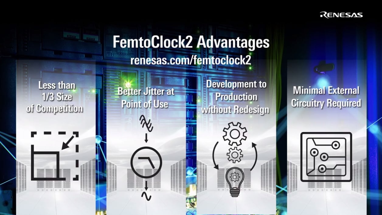
特性
- Jitter below 100fs RMS (10kHz to 20MHz)
- Compliant with ITU-T G.8262 for synchronous Ethernet/OTN (EEC/OEC) and ITU-T G.8262.1 for enhanced synchronous Ethernet/OTN (eEEC/eOEC)
- PLL core consists of fractional-feedback Analog PLL (APLL) which can optionally be steered by a Digital PLL (DPLL)
- Operates from a 25MHz to 80MHz crystal or XO
- APLL frequency independent of input/crystal frequency
- Operates as a frequency synthesizer, jitter attenuator, synchronous equipment slave clock or Digitally Controlled Oscillator (DCO)
- DPLL loop filter programmable from 0.1Hz to 12kHz
- DCO has a tuning granularity of < 1ppb
- Programmable input buffer supports HCSL, LVDS, or two LVCMOS with no external terminations needed
- Input frequencies: 1MHz to 800MHz (250MHz for LVCMOS)
- Reference monitor qualifies/disqualifies input clock
- Programmable status output
- 4 differential/8 LVCMOS outputs
- Any frequency from 10MHz to 1GHz (180MHz for LVCMOS)
- Programmable output buffer supports HCSL (DC-coupled), LVDS/LVPECL/CML (AC-coupled) or two LVCMOS
- Differential output swing is selectable: 400mV to 800mV
- Output clock phase individually adjustable in 100ps steps
- Output Enable input with programmable effect
- Supports up to 1MHz I²C or up to 20MHz SPI serial processor port
- Can configure itself automatically after reset through internal customer-definable One-Time Programmable (OTP) memory with up to four different configurations
- 4mm × 4mm 24-VFQFPN package


RC32504A - Block Diagram
描述
The RC32504A is a small, low-power timing component designed to be placed immediately adjacent to a PHY, switch, ASIC, or FPGA that requires several reference clocks with a jitter performance of less than 100fs. The RC32504A can act as a frequency synthesizer to locally generate the reference clock, a jitter attenuator to perform local clean-up and/or frequency translation of a centrally-supplied reference, a synchronous Ethernet equipment clock to perform passband filtering and clean-up of network-supplied references or as a DCO for frequency margining or OTN clock applications.
产品参数
| 属性 | 值 |
|---|---|
| Inputs (#) | 3 |
| Input Type | Crystal, LVPECL, HCSL, LVDS, CML, LVCMOS |
| Product Category | FemtoClock 2, Ultra-Low Jitter Clocks (<300 fs RMS), Extreme Performance Clocks (<150 fs RMS), Jitter Attenuators, Network Synchronization, PDH and SONET/SDH Clocks, Programmable Clocks |
| Diff. Outputs | 4 |
| Output Type | HCSL, LVDS, LVCMOS |
| Output Voltage (V) | 1.8 |
| Input Freq (MHz) | 1 - 800 |
| Phase Jitter Typ RMS (ps) | 0.079 |
| Output Freq Range (MHz) | 10 - 1000 |
| Fractional Output Dividers (#) | 1 |
| Core Voltage (V) | 1.8V, 3.3V |
| Output Banks (#) | 4 |
| Loop Bandwidth Range (Hz) | 0.1 - 12000 |
| Xtal Freq (KHz) | 25 - 80 |
| Advanced Features | SyncE, DCO, Phase Adjust, External Feedback, Hitless Switching |
| 105°C Max. Case Temp. | 0 |
封装选项
| Pkg. Type | Pkg. Dimensions (mm) | Lead Count (#) | Pitch (mm) |
|---|---|---|---|
| VFQFPN | 4.0 x 4.0 x 0.8 | 24 | 0.5 |
Renesas Boards & Kits
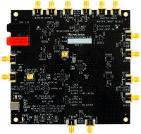
RC32504A-EVK
有效
FemtoClock 2 评估套件
这是用于 RC32504A 和 RC22504A 使用点抖动衰减器和时钟发生器的评估套件。 该电路板装有一个 RC32504A 器件。 RC22504A 在功能上是 RC32504A 的子集,因此该板可用于评估两者中的任意一种或两种器件。 有关产品的更多详细信息,请参阅设备页面。


