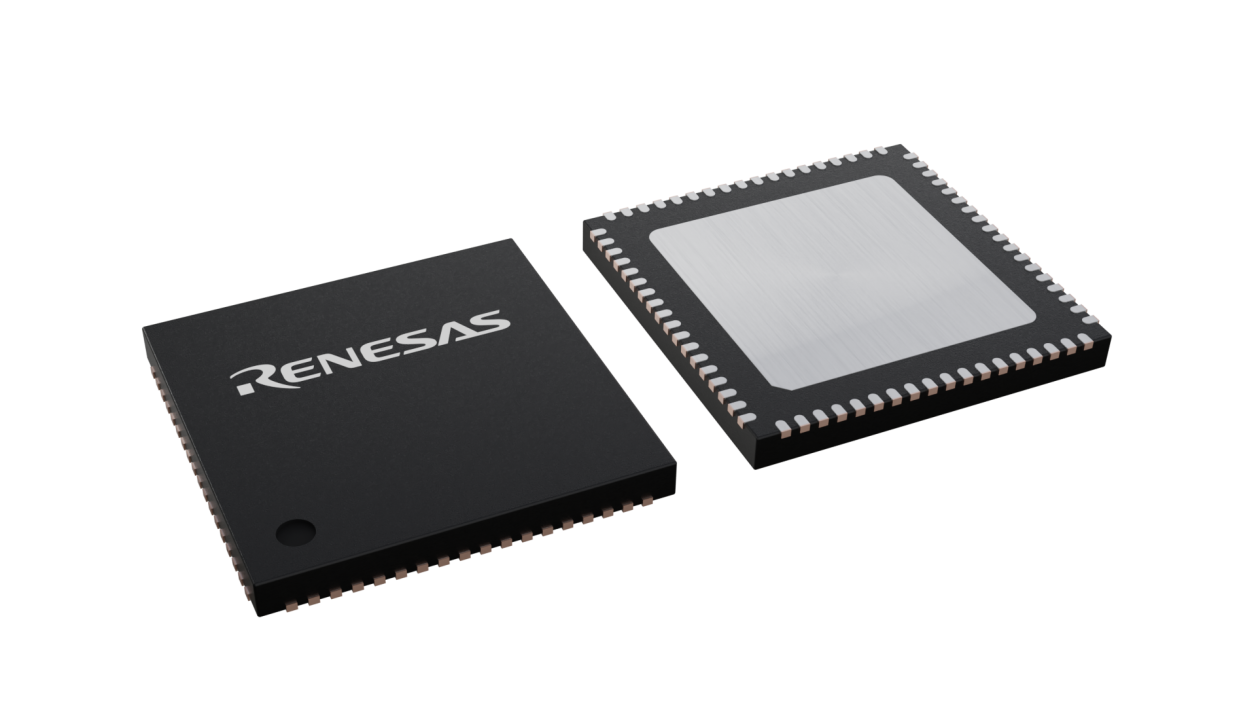
封装信息
| CAD 模型: | View CAD Model |
| Pkg. Type: | VFQFPN |
| Pkg. Code: | NLG72 |
| Lead Count (#): | 72 |
| Pkg. Dimensions (mm): | 10.0 x 10.0 x 1.0 |
| Pitch (mm): | 0.5 |
环境和出口类别
| Moisture Sensitivity Level (MSL) | 3 |
| Pb (Lead) Free | Yes |
| ECCN (US) | EAR99 |
| HTS (US) | 8542.39.0090 |
| RoHS (RC38612A000GN2#BB0) | 英语日文 |
产品属性
| Lead Count (#) | 72 |
| Carrier Type | Tray |
| Moisture Sensitivity Level (MSL) | 3 |
| Qty. per Reel (#) | 0 |
| Qty. per Carrier (#) | 168 |
| Pb (Lead) Free | Yes |
| Pb Free Category | e3 Sn |
| Temp. Range (°C) | -40 to 85°C |
| 105°C Max. Case Temp. | 0 |
| Adjustable Phase | Yes |
| Advanced Features | PWM Encoder/Decoder, ToD, 1PPS, DCO, IEEE 1588, JESD204B, JESD204C, T-BC, T-TSC Class C, eEEC |
| Application | Wireless Baseband Unit (BBU), Distributed Unit (DU), Centralized Unit (CU), Radio Unit (RU) |
| Channels (#) | 6 |
| Core Voltage (V) | 2.5V, 3.3V |
| DPLL Channels (#) | 6 |
| Diff. Inputs | 5 |
| Diff. Outputs | 12 |
| Family Name | ClockMatrix |
| Feedback Divider Resolution (bits) | 48 |
| Fractional Output Dividers (#) | 6 |
| Function | Multi-channel DPLL / DCO |
| Input Freq (MHz) | 0.001 - 1000 |
| Input Redundancy | Input Monitor, Digital holdover, Hitless switch, Phase-slope limiting |
| Input Ref. Divider Resolution (bits) | 4 |
| Input Type | HCSL, LVDS, LVHSTL, LVPECL, SSTL |
| Inputs (#) | 10 |
| JESD204B/C Compliant | Yes |
| Lead Compliant | No |
| Length (mm) | 10 |
| Longevity | 2040 四月 |
| Loop Bandwidth Range (Hz) | 0.0001 - 12000 |
| MOQ | 168 |
| Noise Floor (dBc/Hz) | -158 |
| Output Banks (#) | 6 |
| Output Divider Resolution (bits) | 32 |
| Output Freq Range (MHz) | 5.0E-7 - 1000 |
| Output Skew (ps) | 50 |
| Output Type | HSTL, LVCMOS, LVDS, LVHSTL, LVPECL, LVTTL |
| Output Voltage (V) | 1.2V, 1.5V, 1.8V, 2.5V, 3.3V |
| Outputs (#) | 24 |
| Phase Jitter Typ RMS (ps) | 0.15 |
| Phase Noise Supports GSM | No |
| Pitch (mm) | 0.5 |
| Pkg. Dimensions (mm) | 10.0 x 10.0 x 1.0 |
| Pkg. Type | VFQFPN |
| Product Category | ClockMatrix, JESD204B/C, IEEE 1588, Ultra-Low Jitter Clocks (<300 fs RMS), Jitter Attenuators, Network Synchronization, Programmable Clocks |
| Prog. Interface | I2C, SPI |
| Reference Output | No |
| Spread Spectrum | No |
| Supply Voltage (V) | 3.3 - 3.3, 2.5 - 2.5, 1.8 - 1.8 |
| Synthesis Mode | Fractional, Integer |
| Tape & Reel | No |
| Thickness (mm) | 1 |
| Width (mm) | 10 |
| Xtal Freq (KHz) | 25 - 54 |
有关 RC38612 的资源
描述
The RC38612 RAN synchronizer regenerates and distributes ultra-low jitter; precision timing signals that are locked to IEEE 1588 and Synchronous Ethernet (SyncE) reference sources elsewhere in a system. The device can be used to precisely synchronize IEEE 1588 Time Stamp Units (TSUs) and SyncE ports on wireless baseband, DU, CU, RU, fronthaul or backhaul networks. Digital PLLs (DPLLs) support hitless reference switching between references from redundant timing sources. The device can be used to actively measure and compensate for clock propagation delays across backplanes and across circuit boards to ensure the distribution of accurate time and phase with minimal time error between IEEE 1588 TSUs in a system. The device supports multiple independent timing channels for IEEE 1588 clock synthesis, SyncE clock generation, jitter attenuation, and radio clock generation including SYSREF generation for converters. Input-to-input, input-to-output and output-to-output phase skew can all be precisely managed. The device outputs ultra-low jitter clocks that can directly synchronize SerDes running at up to 28Gbps; as well as CPRI/OBSAI, SONET/SDH ADC/DAC, and IEEE 1588 TSUs.
To see other devices in this product family, visit the ClockMatrix™ Timing Solutions page.


