封装信息
| CAD 模型: | View CAD Model |
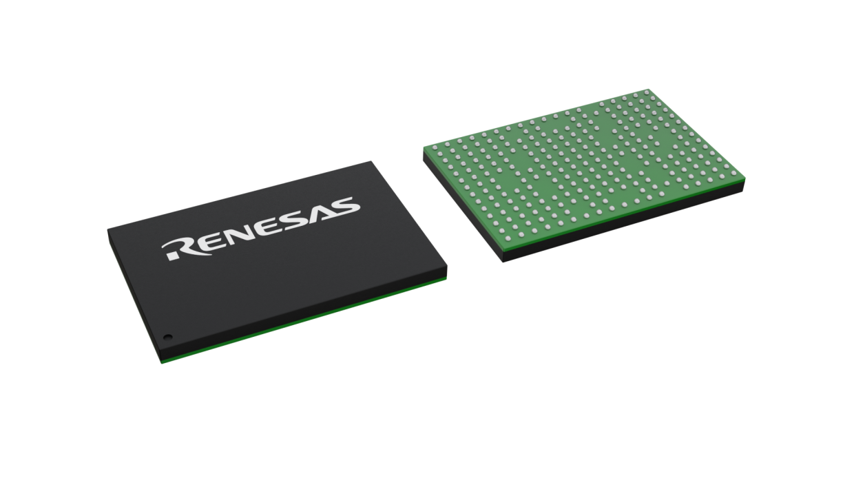
| Pkg. Type: | FCCSP |
| Pkg. Code: | AVG240 |
| Lead Count (#): | 240 |
| Pkg. Dimensions (mm): | 13.5 x 8.7 x 0.9 |
| Pitch (mm): | 0.65 |
环境和出口类别
| Moisture Sensitivity Level (MSL) | 3 |
| Pb (Lead) Free | Yes |
| ECCN (US) | EAR99 |
| HTS (US) | 8542.39.0090 |
产品属性
| Pkg. Type | FCCSP |
| Lead Count (#) | 240 |
| Carrier Type | Reel |
| Moisture Sensitivity Level (MSL) | 3 |
| Qty. per Reel (#) | 3000 |
| Qty. per Carrier (#) | 0 |
| Pb (Lead) Free | Yes |
| Pb Free Category | e1 SnAgCu |
| Temp. Range (°C) | 0 to 70°C |
| Function | DDR5 Gen 4.0 Server RCD |
| Input Voltage Range (V) | 1.06 - 1.16 |
| Length (mm) | 13.5 |
| MOQ | 3000 |
| Pitch (mm) | 0.65 |
| Pkg. Dimensions (mm) | 13.5 x 8.7 x 0.9 |
| Reel Size (in) | 13 |
| Supply Voltage (V) | 1.06 - 1.16 |
| Tape & Reel | Yes |
| Thickness (mm) | 0.9 |
| Width (mm) | 8.7 |
有关 RRG5004 的资源
描述
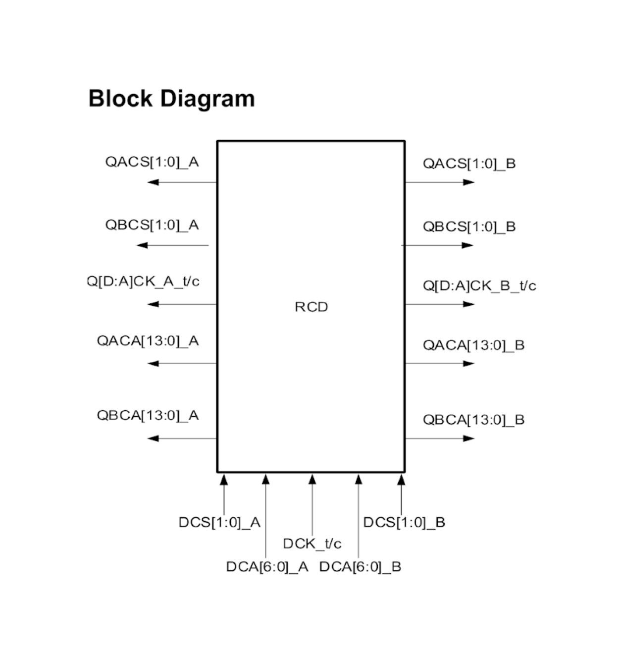
The RRG5004 (Gen 4 RCD) is a registering clock driver used on DDR5 RDIMMs. It supports DDR5 server speeds up to 7200 MT/s. Its primary function is to buffer the Command Address (CA) bus, chip selects, and clock between the host controller and the DRAMs.
- Dual-Channel Design: Operates independently with shared common logic such as clocking, enhancing performance and reliability.
- High-Speed Support: Achieves speeds up to 7200 MT/s, catering to the demands of modern server environments.
- Versatile Compatibility: Supports both x4 and x8 DRAM configurations, providing flexibility for various applications.
- I3C Bus Interface: Facilitates sideband communication with the CPU or motherboard Baseboard Management Controller (BMC), ensuring smooth operations and management.
- Efficient Data Handling: Each channel features a 7-bit double data rate CA bus input, single parity input, two chip-select inputs, and produces two copies of 14-bit single data rate CA bus outputs and chip-select outputs.
- Integrated Clock Management: Common clock input and PLL with separate clock outputs for each DRAM channel, optimizing synchronization and performance.

