特性
- UL2367 Certified as Current Limiter
- File Number: E497808
- Two independent power switches in a single package
- Power supply: 2.5V ≤ VDD ≤ 5.0V
- Input voltage range: 0.9V ≤ VD ≤ VDD
- 14.5mΩ RDSON while supporting 4.5A per channel
- Output voltage slew-rate control by an external capacitor
- Over-temperature protection
- Output discharge circuitry
- Operating Temperature Range: -40 °C to 85 °C

SLG59M1804V
描述
The SLG59M1804V dual N-channel load switch is designed for load switching applications. The device comes with two 4.5A-rated MOSFETs switched on by two ON control pins. The turn-on time for each MOSFET is independently adjusted by an external capacitor.
产品参数
| 属性 | 值 |
|---|---|
| FET Pass Device Type | Dual N-Channel |
| VDD min. (V) | 2.5 |
| VDD max. (V) | 5 |
| VIN Channel 1 min. (V) | 0.9 |
| VIN Channel 1 max. (V) | 5 |
| Input Quiescent Current Channel 1, typ (µA) | 50 |
| Input Quiescent Current Channel 1, max (µA) | 75 |
| Input Quiescent Current when OFF Channel 1, typ (µA) | 0.1 |
| Input Quiescent Current when OFF Channel 1, max (µA) | 1 |
| Input Quiescent Current Channel 2, typ (µA) | 50 |
| Input Quiescent Current Channel 2, max (µA) | 75 |
| Input Quiescent Current when OFF Channel 2, typ (µA) | 0.1 |
| Input Quiescent Current when OFF Channel 2, max (µA) | 1 |
| RDSON (Typ) Channel 1 (mΩ) | 14.5 |
| IDS Channel 1 (A) | 4.5 |
| Enable | Active High |
| Output Voltage Slew Rate set by | Capacitor |
| Discharge Circuit | Yes |
| Undervoltage Protection | No |
| Over Voltage Protection | No |
| Power Good (PG), FAULT indicator | No |
| Reverse current blocking | No |
| Reverse voltage detection | No |
| Over Current Protection (OCP) | Internally Fixed |
| Over Current Protection Setting Range Channel 1 | 6 - 6 |
| Short Circuit Protection | Yes |
| Over Temperature Protection (OTP) | Yes |
| Current Monitor Output | No |
| Internal TVS Surge Protection | No |
| Temp. Range (°C) | -40 to +85°C |
应用
- Ideal for switching ON and OFF S0 +5.0 and 3.3V power rails with associated support circuitry discharges
- Ideal for switching ON and OFF power rails 5.5V or less
- Can use either channel up to 4.5A with a combined maximum current of 8.5A
- Maximum load capacitance of 1000μF for each Channel Source terminal
Renesas Boards & Kits
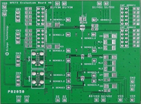
SLG59M1804V Evaluation Board
The SLG59M1804V-EVB board evaluates the SLG59M1804V GreenFET, Dual N-Channel Load Switch.


