
封装信息
| CAD 模型: | View CAD Model |
| Pkg. Type: | TDFN-8 |
| Pkg. Code: | |
| Lead Count (#): | 8 |
| Pkg. Dimensions (mm): | 1.5 x 2.0 mm |
| Pitch (mm): | 0.5 |
环境和出口类别
| Moisture Sensitivity Level (MSL) | 1 |
| Pb (Lead) Free | Yes |
| ECCN (US) | |
| HTS (US) |
产品属性
| Lead Count (#) | 8 |
| Carrier Type | Tape & Reel |
| Moisture Sensitivity Level (MSL) | 1 |
| Pb (Lead) Free | Yes |
| Temp. Range (°C) | -40 to +85°C |
| Country of Assembly | CHINA, TAIWAN |
| Country of Wafer Fabrication | TAIWAN |
| Current Monitor Output | No |
| Discharge Circuit | Yes |
| Enable | Active High |
| FET Pass Device Type | Single N-Channel |
| IDS (A) | 3 |
| IDS Channel 1 (A) | 3 |
| Input Quiescent Current Channel 1, max (µA) | 100 |
| Input Quiescent Current Channel 1, typ (µA) | 70 |
| Input Quiescent Current when OFF Channel 1, max (µA) | 1 |
| Internal TVS Surge Protection | No |
| MOQ | 3000 |
| Output Discharge Circuit | Yes |
| Output Voltage Slew Rate set by | Capacitor |
| Over Current Protection (OCP) | Internally Fixed |
| Over Current Protection Setting Range Channel 1 | 6 - 6 |
| Over Temperature Protection (OTP) | Yes |
| Over Voltage Protection | No |
| Over Сurrent Protection Setting Range (A) | 6 - 6 |
| Parametric Category | Load Switches |
| Pitch (mm) | 0.5 |
| Pkg. Dimensions (mm) | 1.5 x 2.0 mm |
| Pkg. Type | TDFN-8 |
| Power Good (PG), FAULT indicator | No |
| Power Monitor Output | No |
| Price (USD) | $0.44217 |
| Protection Features | Fixed CL, TSD |
| Qty. per Reel (#) | 3000 |
| RDSON (Typ) (mΩ) | 7.8 |
| RDSON (Typ) Channel 1 (mΩ) | 7.8 |
| Ramp Control | Capacitor |
| Reverse current blocking | No |
| Reverse voltage detection | No |
| Short Circuit Protection | Yes |
| Undervoltage Protection | No |
| VD/VIN (Max) | VDD |
| VD/VIN (Min) | 1 |
| VDD Range (V) (V) | 2.5 - 5.5 |
| VDD max. (V) | 5.5 |
| VDD min. (V) | 2.5 |
| VDDl-VDDh (V) | 2.5 - 5.5 |
| VIN Channel 1 max. (V) | 5.5 |
| VIN Channel 1 min. (V) | 1 |
| VIN Range (V) | 1 - 5.5 |
| VIN Range Channel 1 (V) | 1 - 5.5 |
| VIN max. (V) | V5.5 |
| VIN min. (V) | V1 |
| VOUT Discharge Circuit | Yes |
有关 SLG59M308V 的资源
描述
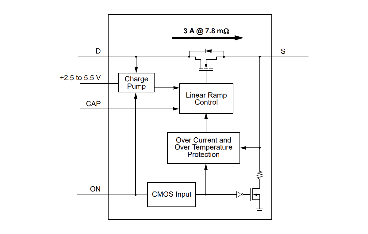
The SLG59M308V is a 7.8mΩ 3A single-channel load switch that can switch 1V to 5.5 V power rails. The product is packaged in an ultra‑small 1.5mm x 2.0mm package.