特性
- Supports GR.1244 Stratum 3 stability in holdover mode
- Compliant with the requirements outlined in Telcordia GR-253-CORE (SONET) & ITU-T G.813/G.8262 (SDH/SONET & SyncE) when paired with a Synchronous Equipment Timing Source (SETS ) device
- Generates up to 8 LVPECL / LVDS/HCSL or 16 LVCMOS output clocks ranging from 8kHz up to 1.0 GHz (diff), 8 kHz to 250 MHz (LVCMOS), that meet jitter limits for 10G up to 100G Ethernet and STM-256/OC-768 applications
- 0.3ps RMS (including spurs), 12 kHz to 20 MHz
- Accepts up to two LVPECL, LVDS, LVHSTL, HCSL or LVCMOS input clocks ranging from 8 kHz up to 875 MHz
- Auto and manual input clock selection with hitless switching
- Clock input monitoring, including support for gapped clocks
- Phase-Slope Limiting and Fully Hitless Switching options to control output phase transients
- Operates from a 10 MHz to 40 MHz fundamental-mode crystal
- Register programmable through I2C / SPI or via external I2C EEPROM
- 8T49N287-993 “Boot from EEPROM”
- 8T49N287-994 “powers up disabled”
- Supported by Timing Commander Software


描述
The 8T49N287 has two fractional feedback PLL’s that can be used as a frequency translators with jitter attenuation or a frequency synthesizers. It is equipped with six integer and two fractional output dividers, allowing the generation of up to eight different output frequencies, ranging from 8 kHz to 1 GHz. Output frequencies can be completely independent of the input frequencies, and up to four of these frequencies can be completely independent of each other. The eight outputs may select among LVPECL, LVDS, HCSL or LVCMOS output levels.
The 8T49N287 is ideal for use in a wide range of equipment, including 10G/40G/100G SONET/SDH and Ethernet network line cards, wireless base station baseband units, broadcast video, carrier Ethernet switches, OTN, or on test and measurement applications. The 8T49N287 can be used in GbE/10GbE/100GbE Synchronous Ethernet line card applications in order to preserve the G.8262 compliance from the Synchronous Equipment Timing Source (SETS) on the timing card.
Renesas’ third generation Universal Frequency Translator family also includes the 8T49N285 (2-in / 1-PLL / 8-out), 8T49N286 (4-in / 2-PLL / 8-out), and the 8T49N242 (2-in / 1-PLL / 4-out). These devices are complemented by the 82P33714 and 82P33731 synchronous equipment timing source (SETS) for Synchronous Ethernet (SyncE) and 10G-40G SyncE, respectively.
To see other devices in this product family, visit the Universal Frequency Translators page.
产品参数
| 属性 | 值 |
|---|---|
| Inputs (#) | 2 |
| Input Type | LVCMOS, LVTTL, HCSL, LVHSTL, LVDS, LVPECL |
| Product Category | FemtoClock NG, IEEE 1588, Ultra-Low Jitter Clocks (<300 fs RMS), Jitter Attenuators, Network Synchronization, PDH and SONET/SDH Clocks, Programmable Clocks, Universal Frequency Translators, FemtoClock NG, Ultra-Low Jitter Clocks (<300 fs RMS), IEEE 1588, Jitter Attenuators, Network Synchronization, PDH and SONET/SDH Clocks, Programmable Clocks, Universal Frequency Translators |
| Diff. Outputs | 8 |
| Output Type | LVCMOS, LVDS, LVPECL, HCSL |
| Output Voltage (V) | 2.5V, 3.3V |
| Input Freq (MHz) | 0.008 - 875 |
| Phase Jitter Typ RMS (ps) | 0.28 |
| Output Freq Range (MHz) | 0.008 - 1000 |
| Fractional Output Dividers (#) | 2 |
| Core Voltage (V) | 2.5V, 3.3V |
| Output Banks (#) | 4 |
| Loop Bandwidth Range (Hz) | 0.5 - 360 |
| Xtal Freq (KHz) | 10000 - 40000 |
| Advanced Features | Programmable Hitless Reference Switching, Fractional-N PLL, External Feedback |
封装选项
| Pkg. Type | Pkg. Dimensions (mm) | Lead Count (#) | Pitch (mm) |
|---|---|---|---|
| VFQFPN | 8.0 x 8.0 x 0.85 | 56 | 0.5 |
Renesas Boards & Kits
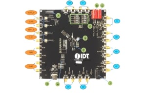
Evaluation Kit for 8T49N285, 8T49N286, 8T49N287
The EVK-UFT285-6-7 is designed to help the customer evaluate the 8T49N285, 8T49N286, and 8T49N287 devices. When the board is connected to a PC running Renesas' Timing CommanderTM software through USB, the device can be configured and programmed to generate frequencies with best-in-class... 阅读详情
