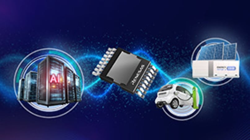
行业趋势正在推动对更高效电源转换的需求。 随着市场对效率、密度和可靠性要求的提高,半导体创新正在被推向人工智能计算的新领域。 这正在改变数据中心以及工业和可再生能源/储能系统的格局。 此外,EV 和 HEV 中的OBC和 DC/DC需要在功率转换方面取得创新进展,以实现更快的充电、更高的续航里程以及更加轻便和经济高效的系统。 在所有这些应用中,速度、效率、外形尺寸(功率密度)和成本是关键痛点。
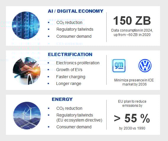
资料来源:Statista “Worldwide Data Created”、各自公司新闻稿、欧盟委员会发布的可持续发展政策文件以及《巴黎协定》
硅在功率转换方面已达到其物理极限。 在当今能够为这些应用提供可行的新架构的半导体材料中,氮化镓 (GaN) 具有最高的能效品质和最低的开关损耗,同时可实现更高的开关速度和更高的频率。 凭借其固有的物理特性,GaN 比传统硅做得更好,也比碳化硅 (SiC) 做得更好。 迄今为止,GaN 的大部分应用都是对可靠性和稳健性要求并不太高的小功率消费类快速充电器。 然而,这种情况正在迅速改变,因为 GaN 带来的高功率密度和高效率可以降低系统成本,成为基础设施、工业、能源和电动汽车等关键市场的必要条件。
可靠性和设计优势
正如新技术经常表现出的情况一样,一种尺寸很少适合所有需求。 然而,对于高功率、高电压 (650V+) 应用的这一关键增长领域,我们认为D-Mode GaN 是优于E-Mode GaN 解决方案,原因如下:
- 完全隔离的栅极,具有更高的稳定性
- 标准栅极驱动避免了复杂的驱动电路、负驱动或定制驱动器
- 具有更高的阈值电压,具有增强的抗噪能力,无需负压驱动
- 饱和电流的温度依赖性较低
- 更好的动态/静态 R(on) 比和较少的第三象限损耗
- 最广泛的封装选项,包括 TO-、SMT 和顶部散热封装
阅读“D-Mode GaN 的基本优势”白皮书,详细了解 D-Mode GaN对比E-Mode GaN 的优势。
瑞萨电子在高压、高功率 GaN 可靠性和认证方面取得了一系列第一,并继续在这个坚实的 SuperGaN® 平台上进行构建,测试要求超出通常标准。 我们最近还发表了一篇会议论文,介绍了运行可靠性测试的正确方法,以确定固有可靠性模式的加速因子,并使用与给定应用中预期的故障模式一致的加速方法。
首先,我们根据 Jedec 47 认证要求、HTRB、HTGB、HTOL要求,对3个lot,每个lot 77 个器件进行了 1000 小时的测试,以确保没有参数故障或重大偏移。 多项测试超越了 AEC-Q101,包括 3000 小时的 HTOL 175°C(对比 150°C)和 -35V 下的 HTGB(对比 20V)。 HTRB,尤其是动态电阻变化是需要控制的关键参数。 如前所述,在高压 HTRB 之后,E-Mode GaN表现出高达 300% 的动态阻抗偏移和高达 30% 的静态阻抗偏移。 最后,短路耐受时间 (SCWT) 等主题需要通过适当驱动 OCP 保护或在芯片上采用内部方法调制 2D 电子气体来管理。 瑞萨电子在这些领域拥有 IP,并展示了高达 5 微秒的 SCWT(参考 APEC 2024 论文)。
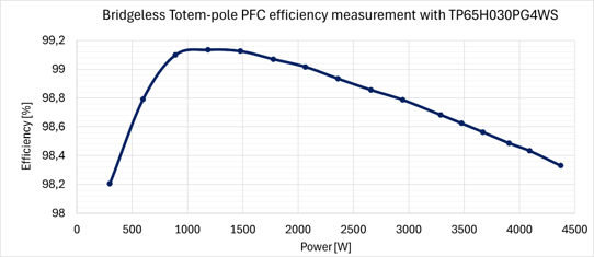
此外,瑞萨电子 GaN 在我们的 PFC 和 DC/DC 转换评估板和参考设计中展示了高达 99% 的效率。
随着 GaN 的不断采用,制造更大直径的晶圆变得必要。 我们还致力于量产 8 英寸晶圆制造的GaN,将我们的高压 GaN 平台中验证的可靠性扩展到更大尺寸的晶圆。 为此,我们最近宣布与美国的 Polar Semiconductor 建立合作伙伴关系 ,除了我们现有的日本高质量 6 英寸晶圆厂外,该公司还将建立第二个晶圆厂。 我们已经在美国、日本和台湾拥有三个外延片制造来源,包括 6 英寸和 8 英寸外延。
瑞萨电子 GaN 采用业内最广泛的封装产品组合之一,从紧凑型 PQFN 到表面贴装、具有顶部和底部散热的高功率封装(TOLT 和 TOLL),以及 TO-220 和 TO-247 等电力电子行业的主力产品,可实现卓越的热管理。 领先的分立式 GaN 封装通常无法与竞争对手的 E-Mode GaN 产品一起使用。
强大的平台和生态系统支持
为了充分发挥GaN 的全部价值,需要利用更强大的生态系统。 我们的主要能力之一是 Renesas Power 生态系统,这是一个广泛的产品组合,在控制器、驱动器和系统方面拥有广泛的专业知识和 IP。 这些功能为我们带来了许多新的 GaN 产品。 此外,这一核心技术使我们能够为 GaN 的关键拓扑开发有针对性的控制器,从图腾柱 PFC 到 LLC,再到 QRF/零电压/零待机电源解决方案和驱动器,包括高电压和低电压、隔离和非隔离,以支持 GaN 的功率级开发。 结合系统解决方案,GaN 的影响力将横跨从数据中心和 AI 处理到工业自动化、电机驱动、机器人和电动汽车市场。
考虑到所有这些要点,并结合前几代产品在该领域超过 3000 亿小时的经验,我们最近推出了我们的 第四代 Plus GaN 平台 ,RDS(on) 和 Rsp 提高了 15%,相关的开关品质因数 (FOM) 提高了 50%。 这些新器件适用于千瓦级应用,如 AI 服务器、储能和 xEV,使设计人员能够以更低的系统成本设计出更高功率密度、更小体积和更高效率的系统。
在 renesas.com/gan-fets 上了解这一新产品组合的所有详细信息。
在“您的高性能系统如何从 GaN 和低压 MOSFET 中受益”博客中阅读有关提高 GaN 对高性能系统的价值的更多信息。