跳转到主要内容
瑞萨电子 (Renesas Electronics Corporation) - June is Pride Month, a month to raise awareness of the rights and the culture of the LGBTQ+ community

描述

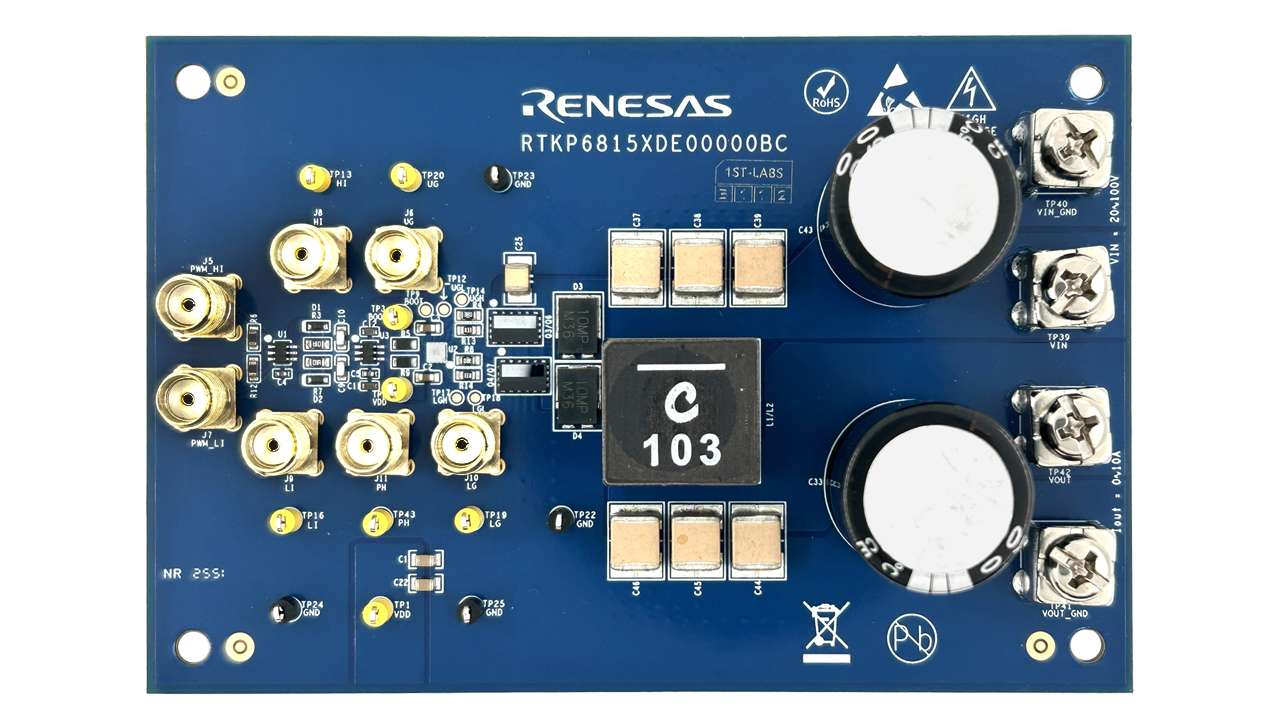
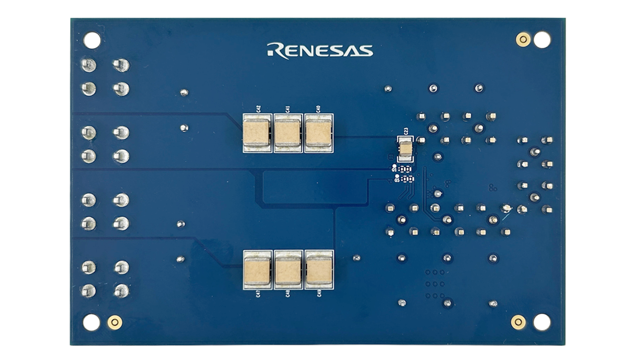
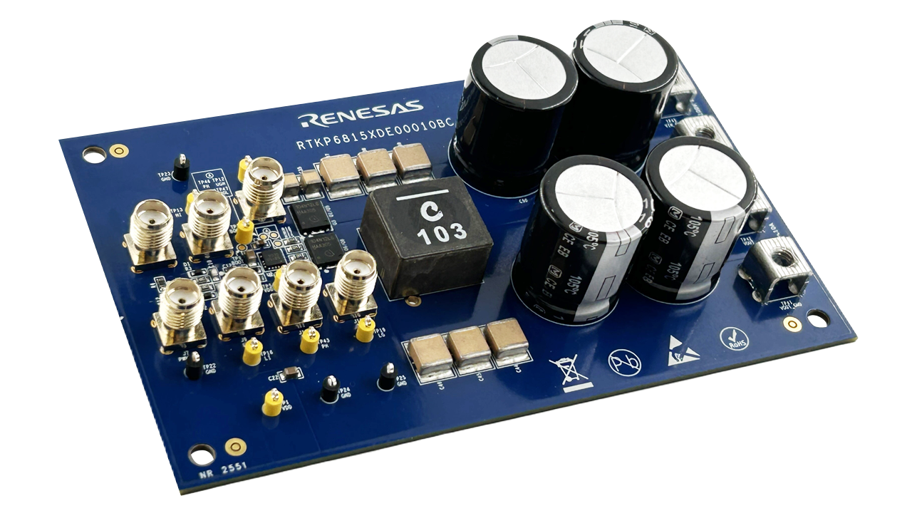
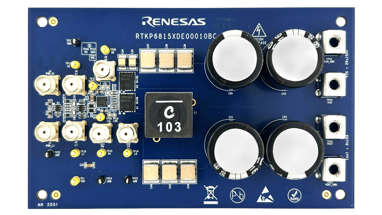
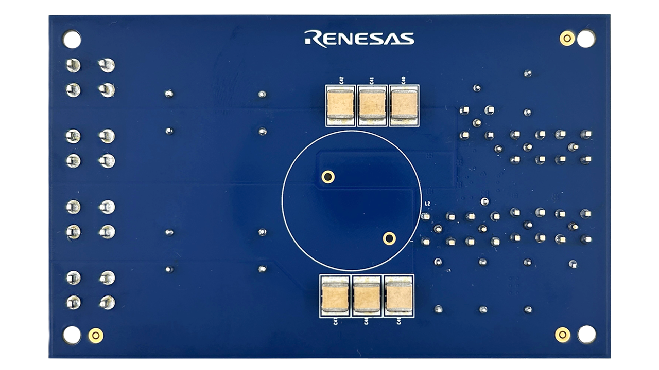
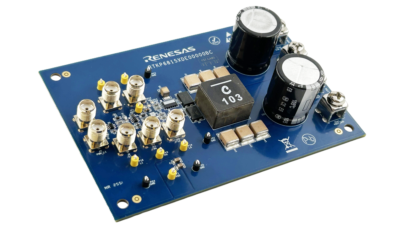
RTKP6815xDE000x0BC 评估板有助于快速、全面地评估 RRP68150 和 RRP68151 半桥驱动器,这两款器件提供 2A 源极和 5.3A 漏极栅极驱动能力。 RTKP6815xDE00000BC 板可有效驱动 GaN FET,而 RTKP6815xDE00010BC 板则在降压系统配置中驱动硅 FET。 每个评估板都集成了两个 GaN FET 或两个逻辑电平 N 通道 MOSFET 以及一个电感电容(LC)滤波器,从而能够在实际工作条件下进行全面的系统级评估。

特性

  • 用于 GaN FET 和 MOSFET 的 2A 源极和 5.3A 漏极驱动器
  • 接受 3.3V/5V 逻辑电平 PWM 输入
  • 传播延迟快:19ns/17ns 典型值
  • 传播延迟匹配出色:1.5ns 典型值
  • 典型上升时间为 4.5ns,典型下降时间为 2.7ns,带 1nF 负载
  • 可单独调节开启和关闭速度
  • 防直通保护(RRP68150)
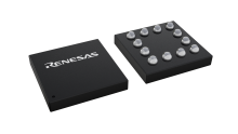
  • RTKP6815xDE00000BC 采用 WLCSP 封装,集成两个 GaN FET
  • RTKP6815xDE00010BC 采用 QFN 封装,集成两个 MOSFET
应用

类型 文档标题 日期
手册 - 开发工具 PDF 2.04 MB
The RTKP6815xDE00000BC and RTKP6815xDE00010BC evaluation boards facilitate a rapid and thorough evaluation of the RRP6815x family devices (RRP68150, RRP68151). This manual provides information about the board design, schematics, bill of materials, and board layout.
PCB 设计文件 ZIP 3.15 MB
The RTKP68150DE00000BC design files include schematics, BOM, PCB layout files, and Gerber artwork for the RTKP68150DE00000BC evaluation board.
PCB 设计文件 ZIP 3.05 MB
The RTKP68150DE00010BC design files include schematics, BOM, PCB layout files, and Gerber artwork for the RTKP68150DE00010BC evaluation board.
PCB 设计文件 ZIP 3.15 MB
The RTKP68151DE00000BC design files include schematics, BOM, PCB layout files, and Gerber artwork for the RTKP68151DE00000BC evaluation board.
PCB 设计文件 ZIP 3.05 MB
The RTKP68151DE00010BC design files include schematics, BOM, PCB layout files, and Gerber artwork for the RTKP68151DE00010BC evaluation board.
5 项目
器件号状态库存Sampleable
RTKP68150DE00000BCActive缺货Available
RTKP68150DE00010BCActive缺货Available
RTKP68151DE00000BCActive缺货Available
RTKP68151DE00010BCActive缺货Available
支持社区

支持社区

在线询问瑞萨电子工程社群的技术人员,快速获得技术支持。
浏览文章

知识库

浏览我们的知识库,获取文章、常见问题解答及其他实用资源。
提交工单

提交工单

需要咨询技术性问题或提供非公开信息吗?