封装信息
| CAD 模型: | View CAD Model |
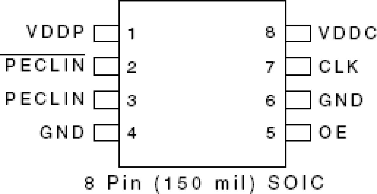
| Pkg. Type: | SOIC |
| Pkg. Code: | DCG8 |
| Lead Count (#): | 8 |
| Pkg. Dimensions (mm): | 4.9 x 3.9 x 1.5 |
| Pitch (mm): | 1.27 |
环境和出口类别
| Moisture Sensitivity Level (MSL) | 1 |
| Pb (Lead) Free | Yes |
| ECCN (US) | EAR99 |
| HTS (US) | 8542.39.0090 |
产品属性
| Lead Count (#) | 8 |
| Carrier Type | Tube |
| Moisture Sensitivity Level (MSL) | 1 |
| Qty. per Reel (#) | 0 |
| Qty. per Carrier (#) | 97 |
| Pb (Lead) Free | Yes |
| Pb Free Category | e3 Sn |
| Temp. Range (°C) | 0 to 70°C |
| Core Voltage (V) | 3.3V, 5V |
| Function | Buffer |
| Input Freq (MHz) | 250 |
| Input Type | LVPECL |
| Inputs (#) | 1 |
| Length (mm) | 4.9 |
| MOQ | 194 |
| Output Banks (#) | 1 |
| Output Freq Range (MHz) | 250 |
| Output Type | LVCMOS |
| Output Voltage (V) | 2.5V, 3.3V, 5V |
| Outputs (#) | 1 |
| Package Area (mm²) | 19.1 |
| Pitch (mm) | 1.27 |
| Pkg. Dimensions (mm) | 4.9 x 3.9 x 1.5 |
| Pkg. Type | SOIC |
| Product Category | Clock Buffers & Drivers |
| Requires Terms and Conditions | Does not require acceptance of Terms and Conditions |
| Tape & Reel | No |
| Thickness (mm) | 1.5 |
| Width (mm) | 3.9 |
有关 508 的资源
描述
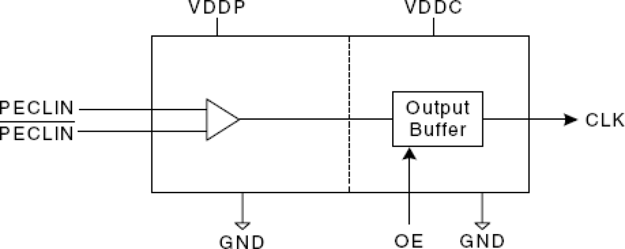
The 508 is the most cost effective way to generate a high quality, high frequency CMOS clock output from a PECL clock input. The 508 has separate VDD supplies for the PECL input buffer and the output buffer, allowing different voltages to be used. For example, the input clock could use a 3.3 V supply while the output operates from 2.5V. The device has an Output Enable pin that tri-states the clock output when the OE pin is taken low. The 508 is a member of IDT's ClockBlocksTM family.


