特性
- Supports PCI Express®TM HCSL Outputs 0.7V current mode differential pair
- Supports LVDS output Levels
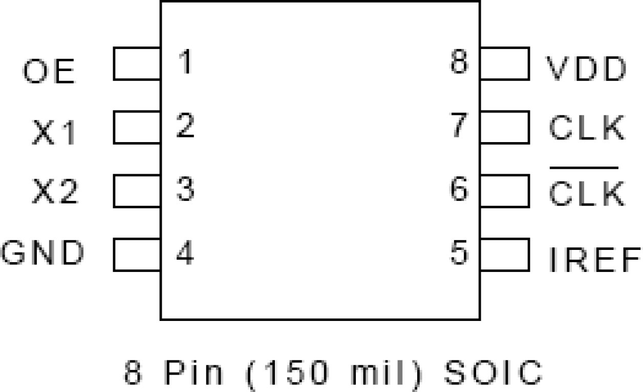
- Packaged in 8-pin SOIC
- RoHS 5 (green) or RoHS 6 (green and lead-free) compliant packaging
- Operating voltage of 3.3V
- Low power consumption
- Input frequency of 25MHz
- Short-term jitter 100ps (peak-to-peak)
- Output Enable via pin selection
- Industrial temperature range available
- For PCIe Gen2 applications, see the 5V41064
- For PCIe Gen3 applications, see the 5V41234
描述
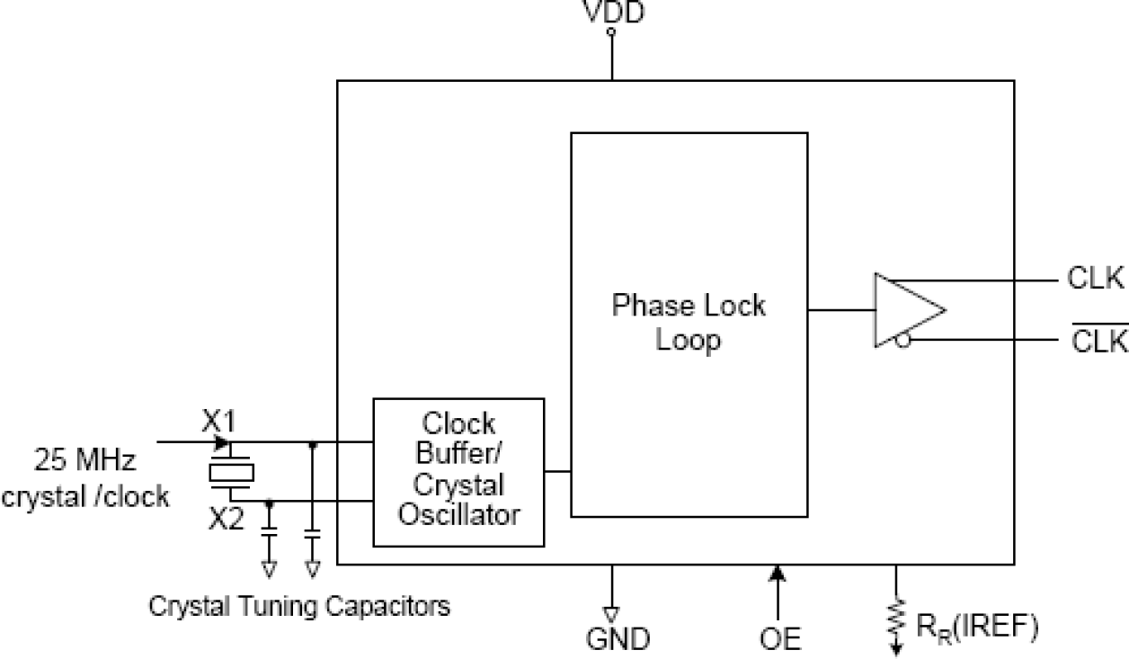
The 557-01 is a clock chip designed for use in PCI Express® cards as a clock source. It provides a pair of differential outputs at 100MHz in a small 8-pin SOIC package. Using Renesas' patented Phase-Locked Loop (PLL) techniques, the device takes a 25MHz crystal input and produces HCSL (Host Clock Signal Level) differential outputs at 100MHz clock frequency. LVDS signal levels can also be supported via an alternative termination scheme.
产品参数
| 属性 | 值 |
|---|---|
| Diff. Outputs | 1 |
| Diff. Output Signaling | HCSL |
| Output Freq Range (MHz) | 100 - 100 |
| Power Consumption Typ (mW) | 182 |
| Supply Voltage (V) | 3.3 - 3.3 |
| Output Type | HCSL |
| Xtal Freq (MHz) | 25 - 25 |
| Diff. Termination Resistors | 4 |
| Package Area (mm²) | 19.1 |
| Battery Backup | No |
| Battery Seal | No |
| CPU Supervisory Function POR | No |
| Crystal Frequency Trimming | No |
| Frequency Out Pin | No |
| Inputs (#) | 1 |
| Input Freq (MHz) | 25 - 25 |
| Input Type | Crystal, LVCMOS |
| Output Banks (#) | 1 |
| Core Voltage (V) | 3.3 |
| Output Voltage (V) | 3.3 |
| Product Category | PCI Express Clocks |
封装选项
| Pkg. Type | Pkg. Dimensions (mm) | Lead Count (#) | Pitch (mm) |
|---|---|---|---|
| SOIC | 4.9 x 3.9 x 1.5 | 8 | 1.27 |
当前筛选条件


