特性
- 1 - 0.7V current mode differential HCSL output pairs
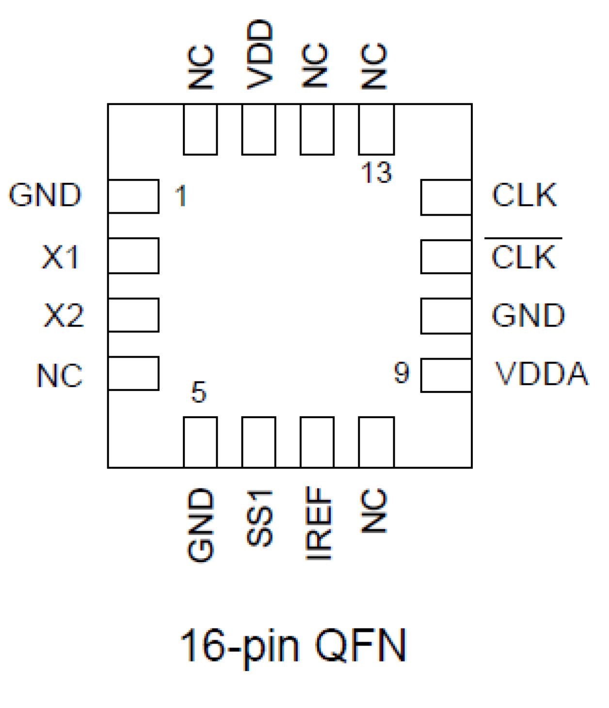
- 16-pin VFQFPN package; very small board footprint
- Spread-spectrum capable; reduces EMI
- Outputs can be terminated to LVDS; can drive a wider variety of devices
- Spread enable via pin selection; no software required to configure device
- Industrial temperature range available; supportsdemanding embedded applications
- Cycle-to-cycle jitter <100 ps
- PCIe Gen2 phase jitter <3.0ps RMS
- PCIe Gen3 phase jitter <1.0ps RMS
描述
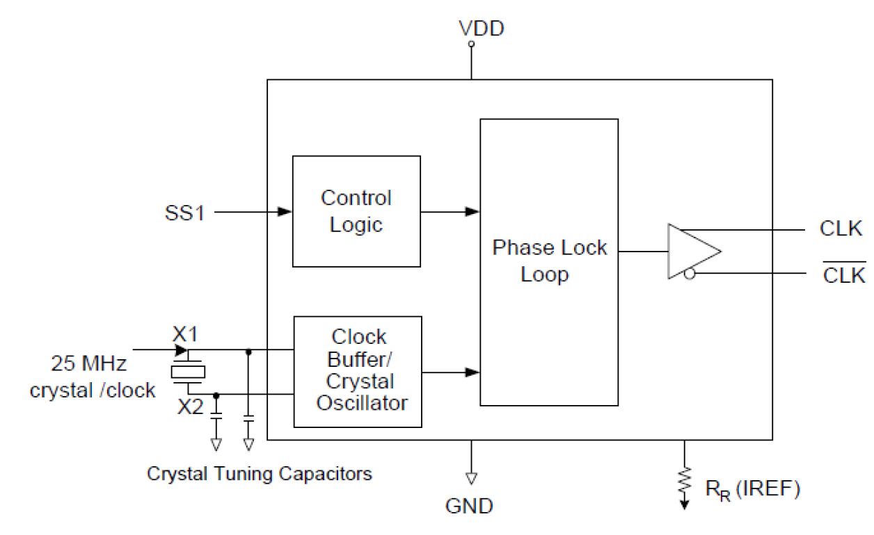
The IDT5V41234 is a PCIe Gen2/3 compliant spread spectrum capable clock generator. The device has 1 differential HCSL output and can be used in communication or embedded systems to substantially reduce electro-magnetic interference (EMI). Spread spectrum can be enabled via a select pin.
产品参数
| 属性 | 值 |
|---|---|
| Diff. Outputs | 1 |
| Diff. Output Signaling | HCSL |
| Output Freq Range (MHz) | 100 - 100 |
| Power Consumption Typ (mW) | 231 |
| Supply Voltage (V) | 3.3 - 3.3 |
| Output Type | HCSL |
| Xtal Freq (MHz) | 25 - 25 |
| Diff. Termination Resistors | 4 |
| Package Area (mm²) | 9 |
| Battery Backup | No |
| Battery Seal | No |
| CPU Supervisory Function POR | No |
| Crystal Frequency Trimming | No |
| Frequency Out Pin | No |
| Inputs (#) | 1 |
| Input Freq (MHz) | 25 - 25 |
| Input Type | Crystal, LVCMOS |
| Output Banks (#) | 1 |
| Core Voltage (V) | 3.3 |
| Output Voltage (V) | 3.3 |
| Product Category | PCI Express Clocks |
封装选项
| Pkg. Type | Pkg. Dimensions (mm) | Lead Count (#) | Pitch (mm) |
|---|---|---|---|
| VFQFPN | 3.0 x 3.0 x 1.0 | 16 | 0.5 |
当前筛选条件


