特性
- 2 differential outputs LVPECL, LVDS, HCSL - or 4 LVCMOS outputs
- 1 additional LVCMOS output
- In-system programmable with 2 independent output frequencies
- Up to 350MHz input/output frequencies
- Stores 4 different configurations in OTP non-volatile memory
- < 100mW core power (at 3.3V)
- < 0.7ps RMS phase jitter (typ.)
- Meets PCIe® Gen 1/2/3, USB 3.0, 1/10 GbE clock requirements
- 1.8V/2.5V/3.3V core and output voltages
- 3mm x 3mm 20-Ld VFQFPN
- -40 °C to +85 °C operating temperature range
- Supported by the Timing Commander™ software tool


描述
The 5P49V5943 is a programmable clock generator intended for high-performance consumer, networking, industrial, computing, and data communications applications. Configurations may be stored in on-chip One-Time Programmable (OTP) memory or changed using the I2C interface. This is Renesas' fifth generation of programmable clock technology (VersaClock® 5). The frequencies are generated from a single input reference clock.
Two select pins allow up to four different configurations to be programmed and accessible using processor GPIOs or bootstrapping. The different selections may be used for different operating modes (full function, partial function, and partial power down), regional standards (US, Japan, Europe), or system production margin testing.
应用
- Ethernet switch/router
- PCI Express 1.0/2.0/3.0
- Broadcast video/audio timing
- Multi-function printer
- Processor and FPGA clocking
- Any-frequency clock conversion
- MSAN/DSLAM/PON
- Fiber channel, SAN
- Telecom line cards
- 1GbE and 10GbE
| Part Number | Status | Samples | Stock | Package | Budgetary Price (USD) | Lead Count (#) | Carrier Type | Moisture Sensitivity Level (MSL) | Qty. per Reel (#) | Qty. per Carrier (#) | Pb (Lead) Free | Pb Free Category | Temp. Range (°C) | Country of Assembly | Country of Wafer Fabrication |
|---|---|---|---|---|---|---|---|---|---|---|---|---|---|---|---|
| 5P49V5943A000NDGI | NRND | Available | Out of Stock | VFQFPN | 20# | Tray | 1 | 0 | 624# | Yes | e3 Sn | -40 to 85°C | |||
| 5P49V5943A000NDGI8 | NRND | N/A | Out of Stock | VFQFPN | 20# | Reel | 1 | 2500# | 0 | Yes | e3 Sn | -40 to 85°C | |||
| 5P49V5943B000NDGI | NRND | Available | In Stock | VFQFPN | 1ku | $3.16 | 20# | Tray | 1 | 0 | 624# | Yes | e3 Sn | -40 to 85°C | TAIWAN | SINGAPORE |
| 5P49V5943B000NDGI8 | NRND | N/A | Out of Stock | VFQFPN | 1ku | $3.16 | 20# | Reel | 1 | 2500# | 0 | Yes | e3 Sn | -40 to 85°C | TAIWAN | SINGAPORE |
- 应用说明英语PDF 1.09 MB R31AN0026EU0102 Rev.1.02 2025年9月06日
- 应用说明英语PDF 187 KB R31AN0065EU0101 Rev.1.01 2023年11月14日
- 手册 - 开发工具英语PDF 1.25 MB 7WDXRDKU4E7E-5-57450 2023年2月02日
- 产品变更通告英语PDF 5.71 MB 2020年6月09日
- 应用说明英语PDF 486 KB 7WDXRDKU4E7E-5-63374 2018年11月01日
- 应用说明英语PDF 717 KB 7WDXRDKU4E7E-5-61645 2017年5月11日
- 应用说明英语PDF 144 KB 7WDXRDKU4E7E-5-59783 2015年12月03日
推荐文档 (1)
数据手册 (1)
- 手册 - 开发工具英语PDF 1.25 MB 7WDXRDKU4E7E-5-57450 2023年2月02日
手册和指南 (2)
- 应用说明英语PDF 1.09 MB R31AN0026EU0102 Rev.1.02 2025年9月06日
- 应用说明英语PDF 187 KB R31AN0065EU0101 Rev.1.01 2023年11月14日
- 应用说明英语PDF 486 KB 7WDXRDKU4E7E-5-63374 2018年11月01日
应用说明和白皮书 (15)
- 产品变更通告英语PDF 5.71 MB 2020年6月09日
- 产品变更通告英语PDF 5.61 MB 2020年1月08日
- 产品变更通告英语PDF 583 KB 7WDXRDKU4E7E-5-61343 2016年12月20日
- 产品变更通告英语PDF 344 KB 7WDXRDKU4E7E-5-59950 2016年2月20日
- 产品变更通告英语PDF 243 KB 7WDXRDKU4E7E-5-59639 2015年10月29日
产品通告(产品变更、EOL 等) (5)
No Results Found.
确保所有关键词拼写正确。
尝试使用更少、不同或更宽泛的词语来改变搜索结果。
如果您使用了筛选器,请考虑取消选择某些筛选器选项以扩大搜索结果。
- 搜索我们丰富的知识库,帮助您解答常见问题
- 前往支持论坛,获取瑞萨电子技术专家和社群的帮助
No Results Found.
确保所有关键词拼写正确。
尝试使用更少、不同或更宽泛的词语来改变搜索结果。
如果您使用了筛选器,请考虑取消选择某些筛选器选项以扩大搜索结果。
- 搜索我们丰富的知识库,帮助您解答常见问题
- 前往支持论坛,获取瑞萨电子技术专家和社群的帮助
No Results Found.
确保所有关键词拼写正确。
尝试使用更少、不同或更宽泛的词语来改变搜索结果。
如果您使用了筛选器,请考虑取消选择某些筛选器选项以扩大搜索结果。
- 搜索我们丰富的知识库,帮助您解答常见问题
- 前往支持论坛,获取瑞萨电子技术专家和社群的帮助
No Results Found.
确保所有关键词拼写正确。
尝试使用更少、不同或更宽泛的词语来改变搜索结果。
如果您使用了筛选器,请考虑取消选择某些筛选器选项以扩大搜索结果。
- 搜索我们丰富的知识库,帮助您解答常见问题
- 前往支持论坛,获取瑞萨电子技术专家和社群的帮助
No Results Found.
确保所有关键词拼写正确。
尝试使用更少、不同或更宽泛的词语来改变搜索结果。
如果您使用了筛选器,请考虑取消选择某些筛选器选项以扩大搜索结果。
- 搜索我们丰富的知识库,帮助您解答常见问题
- 前往支持论坛,获取瑞萨电子技术专家和社群的帮助
No Results Found.
确保所有关键词拼写正确。
尝试使用更少、不同或更宽泛的词语来改变搜索结果。
如果您使用了筛选器,请考虑取消选择某些筛选器选项以扩大搜索结果。
- 搜索我们丰富的知识库,帮助您解答常见问题
- 前往支持论坛,获取瑞萨电子技术专家和社群的帮助
营销资料 (1)
No Results Found.
确保所有关键词拼写正确。
尝试使用更少、不同或更宽泛的词语来改变搜索结果。
如果您使用了筛选器,请考虑取消选择某些筛选器选项以扩大搜索结果。
- 搜索我们丰富的知识库,帮助您解答常见问题
- 前往支持论坛,获取瑞萨电子技术专家和社群的帮助
No Results Found.
确保所有关键词拼写正确。
尝试使用更少、不同或更宽泛的词语来改变搜索结果。
如果您使用了筛选器,请考虑取消选择某些筛选器选项以扩大搜索结果。
- 搜索我们丰富的知识库,帮助您解答常见问题
- 前往支持论坛,获取瑞萨电子技术专家和社群的帮助
Renesas Boards & Kits
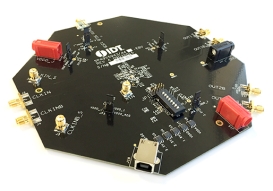
Evaluation Board for 5P49V5943 VersaClock 5
This is the evaluation board for the Renesas 5P49V5943 programmable clock generator. With RMS phase jitter less than 0.7 picoseconds over the full 12kHz to 20MHz integration range, the device meets the stringent jitter requirements of PCI Express® Gen 1/2/3, USB 3.0, and 1G/10G Ethernet.... 阅读详情
筛选
当前筛选条件
软件与工具
按类型筛选
按供应商筛选
样例程序
按应用筛选
按功能筛选
按编译器筛选
按 IDE 筛选
模拟模型
合作伙伴解决方案
- 软件和工具 - 其他英语
- 代码生成器中文Timing Commander™ 是一个基于 Windows™ 的创新软件平台,通过这个平台,系统设计工程师可以通过直观且灵活的图形用户界面 (GUI) 对精密的计时设备进行配置、编程和监控。
No Results Found.
确保所有关键词拼写正确。
尝试使用更少、不同或更宽泛的词语来改变搜索结果。
如果您使用了筛选器,请考虑取消选择某些筛选器选项以扩大搜索结果。
- 搜索我们丰富的知识库,帮助您解答常见问题
- 前往支持论坛,获取瑞萨电子技术专家和社群的帮助
- 软件和工具 - 其他英语
- 代码生成器中文Timing Commander™ 是一个基于 Windows™ 的创新软件平台,通过这个平台,系统设计工程师可以通过直观且灵活的图形用户界面 (GUI) 对精密的计时设备进行配置、编程和监控。
软件与工具 (3)
No Results Found.
确保所有关键词拼写正确。
尝试使用更少、不同或更宽泛的词语来改变搜索结果。
如果您使用了筛选器,请考虑取消选择某些筛选器选项以扩大搜索结果。
- 搜索我们丰富的知识库,帮助您解答常见问题
- 前往支持论坛,获取瑞萨电子技术专家和社群的帮助
模拟模型 (1)
No Results Found.
确保所有关键词拼写正确。
尝试使用更少、不同或更宽泛的词语来改变搜索结果。
如果您使用了筛选器,请考虑取消选择某些筛选器选项以扩大搜索结果。
- 搜索我们丰富的知识库,帮助您解答常见问题
- 前往支持论坛,获取瑞萨电子技术专家和社群的帮助
Lab demonstration and clock jitter measurement showing VersaClock 5. The frequency analyzer shows phase jitter at approximately 575 picoseconds RMS. Presented by Baljit Chandhoke, product manager at IDT. For more information visit the Programmable Clocks page.
This video will show you how to program VersaClock® 5 Low Power Programmable Clock Generator.
Description
IDT's innovative support tool, Timing Commander™, expedites development cycles by empowering customers to program sophisticated timing devices with an intuitive and flexible Graphical User Interface. IDT's Timing Commander is a Windows™-based platform designed to serve user-friendly configuration interfaces, known as personalities, for various IDT products and product families. With a few simple clicks, the user is presented with a comprehensive, interactive block diagram offering the ability to modify desired input values, output values, and other configuration settings. The software automatically makes calculations, reports status monitors, and prepares register settings without the need to reference a datasheet. The tool also automatically loads the configuration settings over USB to an IDT evaluation board for immediate application in the circuit. Once the device has been configured and tuned for optimal system performance, the configuration file can be saved for factory-level programming before shipment. For more information about Timing Commander, visit our Timing Commander page.


