特性
- < 100mW core power (at 3.3V)
- < 0.5ps RMS phase jitter (typical)
- Meets PCIe® Gen 1–4, USB 3.0, 1/10 GbE clock requirements
- Supports both crystal (8MHz – 40MHz) and external clock input (1MHz – 350MHz)
- 4 universal output pairs: LVPECL, LVDS, HCSL, or 8 LVCMOS outputs
- 4 independent frequencies with 0.001MHz – 350MHz output range
- Reference output
- 1.8V/2.5V/3.3V core and output voltages
- 2 programmable I²C addresses allowing multiple devices to be used in the same system
- Up to 4 different configuration sets in OTP non-volatile memory
- Supported by the Renesas IC Toolbox (RICBox) software tool
- Quick sampling and customization process supported by online form submission
- 4mm x 4mm 24-VFQFPN wettable flank package
- AEC-Q100 qualified
- -40°C to +105°C operating temperature range


描述
The 5P49V60 is a member of Renesas' VersaClock® 6E programmable clock generator family. The 5P49V60 is intended for automotive applications such as infotainment, dashboard, video processing, and in-vehicle networking, as well as applications based on PCI-Express or USB 3.0. The reference clock can come from one of the two redundant clock inputs. A glitchless manual switchover function allows one of the redundant clocks to be selected during normal operation.
Configurations may be stored in on-chip One-Time Programmable (OTP) memory or changed using the I²C interface.
产品参数
| 属性 | 值 |
|---|---|
| App Jitter Compliance | PCIe Gen1, PCIe Gen2, PCIe Gen3, PCIe Gen4, PCIe Gen5 |
| Outputs (#) | 5 |
| Output Type | LVCMOS, LVPECL, HCSL, LVDS |
| Output Freq Range (MHz) | 1 - 350 |
| Input Freq (MHz) | 1 - 350 |
| Inputs (#) | 2 |
| Input Type | Crystal, LVCMOS, LVPECL, LVDS, HCSL |
| Output Banks (#) | 4 |
| Core Voltage (V) | 1.8V, 2.5V, 3.3V |
| Output Voltage (V) | 1.8V, 2.5V, 3.3V |
| Product Category | VersaClock 6E, Low Jitter Clocks (<700 fs RMS), Automotive Timing, General Purpose Clocks, Programmable Clocks |
| Selection Criteria | <700 fs RM |
封装选项
| Pkg. Type | Pkg. Dimensions (mm) | Lead Count (#) | Pitch (mm) |
|---|---|---|---|
| VFQFPN | 4.0 x 4.0 x 0.9 | 24 | 0.5 |
应用方框图
 | Android 系统互联车载仪表 采用 Android 系统的汽车驾驶舱,具有无线连接和实时显示功能。 |
 | 通信网关和集成 DVR/DMS 系统 融合 CoGW 与 DVR/DMS 视频处理功能的集成式汽车网关解决方案。 |
 | 高性价比数字集群,配备四通道 AHL 和环视功能 数字集群通过集中信息并通过 AHL 和高效的 PMIC 降低成本来提高安全性。 |
 | 支持触觉反馈的汽车座舱系统 先进的座舱系统,配备新一代触觉反馈技术、BroadLED 驱动器和 PMIC。 |
 | 胎压监测系统 低功耗蓝牙 LE TPMS 设计,集成了 PMIC,可降低成本、缩小尺寸和缩短开发时间。 |
 | 带 AHL 摄像头的泊车辅助系统 具有高清模拟链路的汽车泊车摄像头系统降低了布线成本并保持零延迟。 |
 | 未来 E/E 架构的互联网关 瑞萨电子通过 R-Car SoC、MCU、实时任务和连接支持实现先进的 E/E 汽车架构。 |
 | ADAS 前置摄像头系统 可扩展的 ADAS 前置摄像头系统,具备符合 NCAP 要求的功能和高效深度学习性能。 |
 | 高端驾驶舱和信息娱乐系统解决方案 |
完成您的设计
寻找相关的产品,完善您的设计
Renesas Boards & Kits
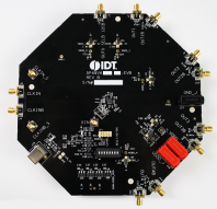
Evaluation Board for 5P49V60 Automotive VersaClock 6E
This is the evaluation board for the 5P49V60 automotive VersaClock® 6E programmable clock generator. With RMS phase jitter of less than 0.5ps over the full 12kHz to 20MHz integration range, the device meets the stringent jitter requirements of PCI Express® Gen 1–3, USB 3.0, and 1G/10G Ethernet.
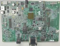
R-Car V4H 系统评测板套装 / White Hawk
White Hawk 是一款适用于 R-Car V4H 的评估套件,可使用 R-Car V4H 来评估系统并用来开发操作系统、设备驱动器和应用程序。 使用 White Hawk 评估套件可让开发人员高效地执行所需任务,例如评估 R-Car V4H 系统性能,从而大大缩短产品开发的周期。
该板支持多摄像头输入,包括4K高分辨率输入、4K 显示输出、音频输出、网络通信接口和适用于多 ECU 并行运行的 PCIe Gen4。
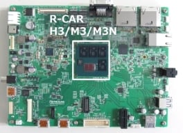
高端驾驶舱和信息娱乐系统解决方案 R-Car H3、M3 开发板/Salvator-XS
R-Car(H3/M3/M3N)系统级封装(SiP)和时钟发生器的组合可提供高效率,同时支持多种显示输出和高质量性能,因此十分适合可扩展的驾驶舱和信息娱乐系统解决方案。
