
特性
- Operating frequency range: 0-1000 MHz
- Output skew: <25ps (maximum)
- Duty cycle distortion: <125ps (maximum)
- Selectable inputs
- Hot insertable and over-voltage tolerant inputs
- 3.3V/2.5V LVTTL, HSTL, LVPECL, CML or LVDS input interface
- Power-down mode
- 2.5V voltage supply
- -40°C to 85°C ambient operating temperature
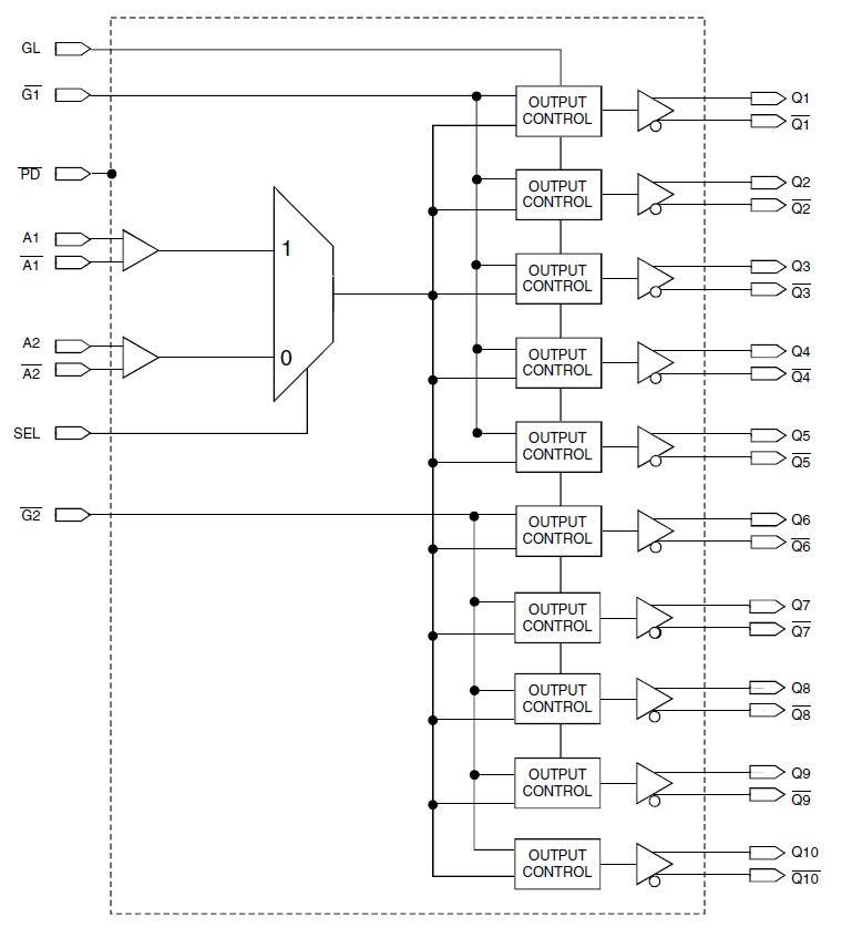
5T9310 - Block Diagram
描述
The 5T9310 is a low skew, 1-to-10 differential LVDS clock fanout buffer. The device has two selectable inputs. The inputs accept LVDS, HSTL, CML, LVPECL and single-ended signals such as 3.3V/2.5V LVCMOS/LVTTL. The 5T9310 outputs can be asynchronously enabled/disabled. When disabled, the outputs will drive to the value selected by the GL pin. Multiple power and grounds reduce noise.
| Part Number | Status | Samples | Stock | Package | Lead Count (#) | Temp. Grade | Pb (Lead) Free | Carrier Type |
|---|---|---|---|---|---|---|---|---|
| 5T9310NLGI | Obsolete | N/A | Out of Stock | VFQFPN | 40# | I | Yes | Tray |
| 5T9310NLGI8 | Obsolete | N/A | Out of Stock | VFQFPN | 40# | I | Yes | Reel |
加载中
请登录后开启订阅
- 应用说明英语PDF 495 KB 7WDXRDKU4E7E-5-57312 2014年5月12日
- 应用说明英语PDF 120 KB 7WDXRDKU4E7E-5-57289 2014年5月06日
- 应用说明英语PDF 160 KB 7WDXRDKU4E7E-5-57287 2014年5月06日
- 应用说明英语PDF 180 KB 7WDXRDKU4E7E-5-57283 2014年5月06日
- 产品变更通告英语PDF 24 KB 7WDXRDKU4E7E-5-41812 2012年11月14日
- 产品变更通告英语PDF 80 KB 7WDXRDKU4E7E-5-41813 2004年12月14日
No Results Found.
检查拼写
确保所有关键词拼写正确。
确保所有关键词拼写正确。
调整关键词
尝试使用更少、不同或更宽泛的词语来改变搜索结果。
尝试使用更少、不同或更宽泛的词语来改变搜索结果。
查看筛选器
如果您使用了筛选器,请考虑取消选择某些筛选器选项以扩大搜索结果。
如果您使用了筛选器,请考虑取消选择某些筛选器选项以扩大搜索结果。
需要帮助?
- 搜索我们丰富的知识库,帮助您解答常见问题
- 前往支持论坛,获取瑞萨电子技术专家和社群的帮助
No Results Found.
检查拼写
确保所有关键词拼写正确。
确保所有关键词拼写正确。
调整关键词
尝试使用更少、不同或更宽泛的词语来改变搜索结果。
尝试使用更少、不同或更宽泛的词语来改变搜索结果。
查看筛选器
如果您使用了筛选器,请考虑取消选择某些筛选器选项以扩大搜索结果。
如果您使用了筛选器,请考虑取消选择某些筛选器选项以扩大搜索结果。
需要帮助?
- 搜索我们丰富的知识库,帮助您解答常见问题
- 前往支持论坛,获取瑞萨电子技术专家和社群的帮助
应用说明和白皮书 (12)
- 产品变更通告英语PDF 790 KB 7WDXRDKU4E7E-5-57153 2014年4月08日
- 产品变更通告英语PDF 24 KB 7WDXRDKU4E7E-5-41812 2012年11月14日查看更多 (8)
产品通告(产品变更、EOL 等) (8)
No Results Found.
检查拼写
确保所有关键词拼写正确。
确保所有关键词拼写正确。
调整关键词
尝试使用更少、不同或更宽泛的词语来改变搜索结果。
尝试使用更少、不同或更宽泛的词语来改变搜索结果。
查看筛选器
如果您使用了筛选器,请考虑取消选择某些筛选器选项以扩大搜索结果。
如果您使用了筛选器,请考虑取消选择某些筛选器选项以扩大搜索结果。
需要帮助?
- 搜索我们丰富的知识库,帮助您解答常见问题
- 前往支持论坛,获取瑞萨电子技术专家和社群的帮助
No Results Found.
检查拼写
确保所有关键词拼写正确。
确保所有关键词拼写正确。
调整关键词
尝试使用更少、不同或更宽泛的词语来改变搜索结果。
尝试使用更少、不同或更宽泛的词语来改变搜索结果。
查看筛选器
如果您使用了筛选器,请考虑取消选择某些筛选器选项以扩大搜索结果。
如果您使用了筛选器,请考虑取消选择某些筛选器选项以扩大搜索结果。
需要帮助?
- 搜索我们丰富的知识库,帮助您解答常见问题
- 前往支持论坛,获取瑞萨电子技术专家和社群的帮助
No Results Found.
检查拼写
确保所有关键词拼写正确。
确保所有关键词拼写正确。
调整关键词
尝试使用更少、不同或更宽泛的词语来改变搜索结果。
尝试使用更少、不同或更宽泛的词语来改变搜索结果。
查看筛选器
如果您使用了筛选器,请考虑取消选择某些筛选器选项以扩大搜索结果。
如果您使用了筛选器,请考虑取消选择某些筛选器选项以扩大搜索结果。
需要帮助?
- 搜索我们丰富的知识库,帮助您解答常见问题
- 前往支持论坛,获取瑞萨电子技术专家和社群的帮助
No Results Found.
检查拼写
确保所有关键词拼写正确。
确保所有关键词拼写正确。
调整关键词
尝试使用更少、不同或更宽泛的词语来改变搜索结果。
尝试使用更少、不同或更宽泛的词语来改变搜索结果。
查看筛选器
如果您使用了筛选器,请考虑取消选择某些筛选器选项以扩大搜索结果。
如果您使用了筛选器,请考虑取消选择某些筛选器选项以扩大搜索结果。
需要帮助?
- 搜索我们丰富的知识库,帮助您解答常见问题
- 前往支持论坛,获取瑞萨电子技术专家和社群的帮助
No Results Found.
检查拼写
确保所有关键词拼写正确。
确保所有关键词拼写正确。
调整关键词
尝试使用更少、不同或更宽泛的词语来改变搜索结果。
尝试使用更少、不同或更宽泛的词语来改变搜索结果。
查看筛选器
如果您使用了筛选器,请考虑取消选择某些筛选器选项以扩大搜索结果。
如果您使用了筛选器,请考虑取消选择某些筛选器选项以扩大搜索结果。
需要帮助?
- 搜索我们丰富的知识库,帮助您解答常见问题
- 前往支持论坛,获取瑞萨电子技术专家和社群的帮助
No Results Found.
检查拼写
确保所有关键词拼写正确。
确保所有关键词拼写正确。
调整关键词
尝试使用更少、不同或更宽泛的词语来改变搜索结果。
尝试使用更少、不同或更宽泛的词语来改变搜索结果。
查看筛选器
如果您使用了筛选器,请考虑取消选择某些筛选器选项以扩大搜索结果。
如果您使用了筛选器,请考虑取消选择某些筛选器选项以扩大搜索结果。
需要帮助?
- 搜索我们丰富的知识库,帮助您解答常见问题
- 前往支持论坛,获取瑞萨电子技术专家和社群的帮助
- 产品简述英语PDF 378 KB 7WDXRDKU4E7E-6-1169 2012年8月14日
营销资料 (3)
No Results Found.
检查拼写
确保所有关键词拼写正确。
确保所有关键词拼写正确。
调整关键词
尝试使用更少、不同或更宽泛的词语来改变搜索结果。
尝试使用更少、不同或更宽泛的词语来改变搜索结果。
查看筛选器
如果您使用了筛选器,请考虑取消选择某些筛选器选项以扩大搜索结果。
如果您使用了筛选器,请考虑取消选择某些筛选器选项以扩大搜索结果。
需要帮助?
- 搜索我们丰富的知识库,帮助您解答常见问题
- 前往支持论坛,获取瑞萨电子技术专家和社群的帮助
No Results Found.
检查拼写
确保所有关键词拼写正确。
确保所有关键词拼写正确。
调整关键词
尝试使用更少、不同或更宽泛的词语来改变搜索结果。
尝试使用更少、不同或更宽泛的词语来改变搜索结果。
查看筛选器
如果您使用了筛选器,请考虑取消选择某些筛选器选项以扩大搜索结果。
如果您使用了筛选器,请考虑取消选择某些筛选器选项以扩大搜索结果。
需要帮助?
- 搜索我们丰富的知识库,帮助您解答常见问题
- 前往支持论坛,获取瑞萨电子技术专家和社群的帮助
加载中
筛选
当前筛选条件
软件与工具
按类型筛选
按供应商筛选
样例程序
按应用筛选
按功能筛选
按编译器筛选
按 IDE 筛选
模拟模型
Partner Solutions
No Results Found.
检查拼写
确保所有关键词拼写正确。
确保所有关键词拼写正确。
调整关键词
尝试使用更少、不同或更宽泛的词语来改变搜索结果。
尝试使用更少、不同或更宽泛的词语来改变搜索结果。
查看筛选器
如果您使用了筛选器,请考虑取消选择某些筛选器选项以扩大搜索结果。
如果您使用了筛选器,请考虑取消选择某些筛选器选项以扩大搜索结果。
需要帮助?
- 搜索我们丰富的知识库,帮助您解答常见问题
- 前往支持论坛,获取瑞萨电子技术专家和社群的帮助
No Results Found.
检查拼写
确保所有关键词拼写正确。
确保所有关键词拼写正确。
调整关键词
尝试使用更少、不同或更宽泛的词语来改变搜索结果。
尝试使用更少、不同或更宽泛的词语来改变搜索结果。
查看筛选器
如果您使用了筛选器,请考虑取消选择某些筛选器选项以扩大搜索结果。
如果您使用了筛选器,请考虑取消选择某些筛选器选项以扩大搜索结果。
需要帮助?
- 搜索我们丰富的知识库,帮助您解答常见问题
- 前往支持论坛,获取瑞萨电子技术专家和社群的帮助
No Results Found.
检查拼写
确保所有关键词拼写正确。
确保所有关键词拼写正确。
调整关键词
尝试使用更少、不同或更宽泛的词语来改变搜索结果。
尝试使用更少、不同或更宽泛的词语来改变搜索结果。
查看筛选器
如果您使用了筛选器,请考虑取消选择某些筛选器选项以扩大搜索结果。
如果您使用了筛选器,请考虑取消选择某些筛选器选项以扩大搜索结果。
需要帮助?
- 搜索我们丰富的知识库,帮助您解答常见问题
- 前往支持论坛,获取瑞萨电子技术专家和社群的帮助
模拟模型 (1)
No Results Found.
检查拼写
确保所有关键词拼写正确。
确保所有关键词拼写正确。
调整关键词
尝试使用更少、不同或更宽泛的词语来改变搜索结果。
尝试使用更少、不同或更宽泛的词语来改变搜索结果。
查看筛选器
如果您使用了筛选器,请考虑取消选择某些筛选器选项以扩大搜索结果。
如果您使用了筛选器,请考虑取消选择某些筛选器选项以扩大搜索结果。
需要帮助?
- 搜索我们丰富的知识库,帮助您解答常见问题
- 前往支持论坛,获取瑞萨电子技术专家和社群的帮助


