特性
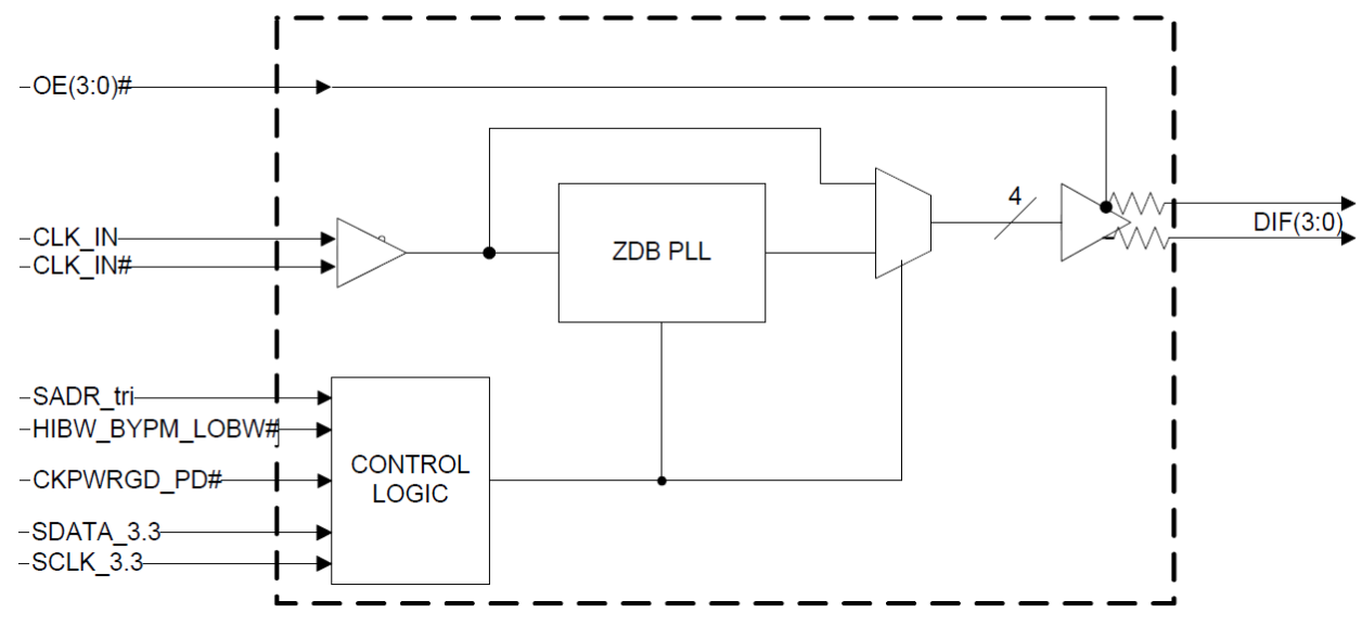
- Integrated terminations provide differential Zo = 100Ω: reduced component count and board space
- 1.8V operation: minimal power consumption
- OE# pins: support DIF power management
- HCSL compatible differential input: can be driven by common clock sources
- LP-HCSL differential clock outputs: reduced power and board space
- Programmable Slew rate for each output: allows tuning for various line lengths
- Programmable output amplitude: allows tuning for various application environments.
- Pin/Software selectable PLL bandwidth and PLL bypass: minimize phase jitter for each application
- Outputs blocked until PLL is locked: clean system start-up
- Software selectable 50MHz or 125MHz PLL operation: useful for Ethernet applications
- Configuration can be accomplished with strapping pins: SMBus interface is not required for device control
- 3.3V tolerant SMBus interface works with legacy controllers
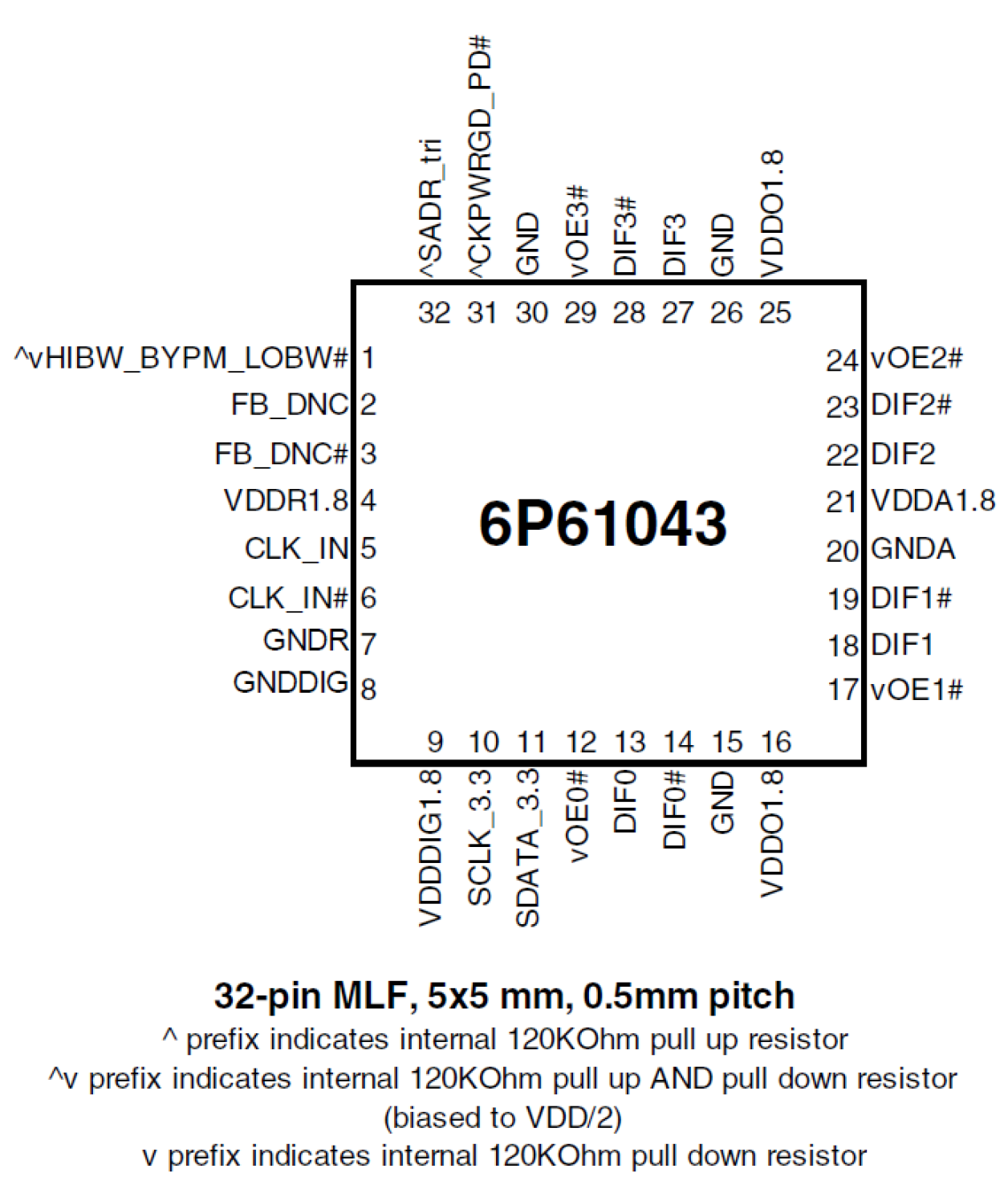
- Space saving 32-pin 5mm x 5mm MLF: minimal board space
- Selectable SMBus addresses: multiple devices can easily share an SMBus segment
描述
The 6P61043 is a 4-output very-low power buffer for 100MHz PCIe Gen 1, Gen 2, and Gen 3 applications with integrated output terminations providing Zo = 100Ω for Freescale Systems. The device has four output enables for clock management and three selectable SMBus addresses.
产品参数
属性 | 值 |
---|---|
Architecture | Common, SRNS |
App Jitter Compliance | PCIe Gen1, PCIe Gen2, PCIe Gen3 |
Diff. Outputs | 4 |
Diff. Output Signaling | LP-HCSL |
Diff. Inputs | 1 |
Power Consumption Typ (mW) | 65 |
Supply Voltage (V) | - |
Advanced Features | HW PLL mode control, Multiple SMBus addresses |
封装选项
Pkg. Type | Pkg. Dimensions (mm) | Lead Count (#) | Pitch (mm) |
---|---|---|---|
VFQFPN | 5.0 x 5.0 x 0.9 | 32 | 0.5 |
当前筛选条件
筛选
软件与工具
样例程序
模拟模型
A detailed overview of IDT's full-featured PCI Express (PCIe) clock and timing solutions. The presentation addresses PCIe Gen 1, Gen 2, Gen 3, and Gen 4 architectures and how IDT's industry-leading solutions provide all the functions, features, and performance required by the application.
Presented by Ron Wade, System Architect at IDT. For more information visit the PCIe clocks page.
TRANSCRIPT
Hi there. This is the first in the five-part series on IDT's new full-featured PCIe clock family. The first part in the series will be a family overview. There will also be a part on the clock generators, another section covering the clock buffers, a fourth section that will deal with the clock multiplexers and finally, a fifth section covering some of the applications for the full-featured PCIe clocks. So let's jump right into the family overview.
So PCI Express is evolving. There are two major things happening in PCI Express these days. One is the PCIe Gen4 specification is moving toward 0.9 drafts stage. And Gen4 is going to bring 16 Gbps data transfers to the architecture or to the PCI Express world. And then there's also going to be two new architectures which are supported in a non-specific way. The two architectures are the separate reference no spread--or SRNS--and the separate reference independence spread--or SRIS--clock architectures. These are going to be supported in the PCI Express Gen4 specification but there will be no explicit specifications on the reference clocks. So what the phrase is, is that SRNS and SRIS clocking will be implementation dependent. And what that means is that there's not gonna be an explicit reference clock jitter specification. And that means that IDT will need to work with the SOC vendors to ensure interoperability. And regardless of whether there's an explicit specification or not, IDT delivers solutions for these architectures and increasing performance requirements and we have always done so.
So in terms of the IDT's PCIe clock families, there are three major families. The focus of these series of presentations is on the full-featured PCIe, which you see on the left of your screen. We've just introduced the new L-series parts to production, which are the 3.3V devices that have the best performance - PCI Gen1 through 4, and also SRNS and SRIS support. And those follow the very successful 1.8V V-series and the 1.5V U-series parts which have been in the market for a couple of years supporting Gen1 through 3. The other specs and the Gen4 common clock spec are being evaluated against these parts to see if they will be able to do Gen4 or not. And so those other specs are TBD. The other family that we have is the PhiClock family, which is PhiClock plus PCIe in this case, where we add some less than 300 femtosecond RMS high-performance SerDes clocks or PhiClocks and then also provide some PCI Express Gen1 through 4 clocks.
Then the last family is when you really need to go smaller and you don't need all the features, you want a simpler board layout and you have very tight space constraints, is the micro-PCIe family which will be the subject of another presentation. And we're defining smaller as in micro-PCIe as any device that is in a 3x3 millimeter or smaller package.
So the common features of IDT's full-featured PCIe family are as follows. You have an Output Enable pin for every PCIe clock, you have Spread Spectrum Clocking capability and compatibility across every part in the family. On the clock generators, there is a reference output which can save you an XO in your system. And then to make it really simple to use the parts, you have--on the clock generators--you have pin control of three different spread amounts including spread off. And you also have on the zero-delay buffers pin control of the PLL bandwidth, whether you want it to be high bandwidth, low bandwidth or the PLL bypassed, that is all done from a single pin.
The other common feature is multiple, pin selectable SMBus addresses. So the clock generators have a choice of two SMBus addresses, the buffers have a choice of three SMBus addresses and those five addresses do not overlap. So you can have up to five of these devices on a single SMBus segment. The other common feature is that we use low power, and some people refer to this as push-pull, but we use low-power HCSL outputs on all the parts and they are offered with a choice of 100 ohm integrated terminations or 85 ohm integrated terminations. And all the parts in the full-featured family are between 2.5 mm x 2.5 mm up to 6 mm x 6 m. They all offer I-temp operation and the most power consuming part consumes 211 mW, so they are very power efficient.
So, the 3.3V full-featured PCIe clock family, which is the newest one, provides the basic functions you need for clocking, provides a clock generator function, provides both zero delay and fanout buffers, and provides a clock muxing function. And the muxes are two inputs with different numbers of outputs. In the 3.3V family, it's a 2-input and 4-output mux.
So the family has performance. The 3.3V family is PCIe Gen1, 2, 3, 4 common clocked compliant. It also supports the SRNS and SRIS architectures. You've got flexibility in the family where you can right-size the part for your design because we provide from two to nine outputs. Again, the 3.3V family does allow factory OTP customization if you have a particular setting that you would like to adjust, whether it's slew rate, output impedance, polarity of control signals, or even on the clock generators, maybe you prefer to run from a 20 MHz or 24 MHz reference clock instead of 25. That can easily be OTP into the parts.
We also have easy AC coupling to other logic standards such LVPECL, LVDS, and CML. There's SMBus programmability for the signal integrity and functionality. And again that can be OTP customized for your particular needs. And then we have 1.5 and 1.8V versions of the parts available for the more power-conscious applications that might be out there. As far as 3.3V size and power, this family ranges from a 4x4 mm at the smallest end to a 6x6 mm QFN in the largest part. These save up to 53% board area compared to IDT's legacy 3.3V current mode devices such as the 9DB803 for instance.
The integrated terminations allow you to save up to 36 resistors and that 36 resistors represent 62 mm2 of board area. So really great for space constrained designs. And then power-wise, the low power HCSL outputs allow up to an 80% power savings with the 3.3V parts. If you can use 1.5 or 1.8 in your design you can save even more power. The parts are easy to use because as shown earlier, the basic functions are controlled by hardware pins. So you do not need to use the SMBus for most applications. And we do have the individual OE pin on each PCIe output.
So the 3.3V full-featured PCIe clocks support Gen1, 2, 3, 4 common clock, SRIS and SRNS. It is a family of parts with a clock generator, fanout buffers, zero delay buffers, and clock multiplexers. And it supports both 100 ohm environments and 85 ohm environments without any external components. The numbering scheme is really easy. All parts start with a 9. And if you're looking for a generator it's a 9FG, the FG stands for frequency generator actually. If you're looking for a buffer, it's 9DB, for differential buffer. And if you're looking for a mux, it's 9DM, for differential mux. And then the operating voltage is the fourth character in the part number, L is for 3.3V, which stands for Low power. The V indicates 1.8V, or Very low power. And then the U indicates 1.5V, or Ultra-Low power.
The next two digits then provide the number of PCIe clock output pairs. So arranging from 1 all the way up to 9 currently. So that's the number of outputs. And then finally, the next to last digit indicates the output impedance. So a 33-ohm output impedance would have a 3 as the next to last digit. And then the device variant would be like 31, 32, 33, 34, etc. 100ohm output impedance has the next to last digit as a 4. And you would have 41, 42, 43, 44, etc. And then finally the 85-ohm output impedance starts with a 5 and that would be like 51, 52, 53, etc. That's it for the PCI Express family overview. Thank you for watching.
This is the first video in our PCIe series. In this video, we define PCIe architectures, focusing on common and separate clock architectures. Watch the rest of the video series below where Ron will cover the impact of different timing architectures.
Watch the Video Series Below
In this episode, Ron Wade from IDT (acquired by Renesas) explains PCIe common clocking and its impact on timing solutions. Learn about using a single clock source, fan-out buffers, and the considerations for spread spectrum and non-spread spectrum clocking in PCIe systems.
Watch the Video Series Below
- PCIe Clocking Architectures (Common and Separate)
- PCIe Separate Reference without Spread Clock Architecture
- PCIe Separate Reference Clock With Independent Spread (SRIS) Architecture Overview
Transcript
Hi, this is Ron Wade again with IDT. Today in this little episode we're gonna talk about PCI Express common clocking and its impact on the timing solutions that you would use in the system. So, as the name implies, common clocking says that all of the clocks come from one source. In this case it's a PLL. It may be spreading, it may not, but very seldom do you get all of your clocks from one device, so you'll need some sort of fan out buffers to distribute extra copies of the PCI Express clocks.
And while it's still a common clock, now we have to take into account whether we're using spread spectrum or whether we're using non-spread spectrum. If we are not using SFC, then we can fan out to these buffers here, and this could be a ZDB with a PLL inside, or it could be a fan out buffer, or it could be a part where you select between the two. Without spread spectrum, I can put this buffer in PLL mode or ZDB mode, it doesn't really matter and I don't violate the common clock requirement from the PCI Express sig. Same with this guy, it could be a fan out buffer or a PLL, ZDB, it doesn't really matter.
Things get really interesting though when spread spectrum is in use. When spread spectrum is in use then I have to have...this is my common clock. With spread spectrum in use, these have to be in fan out buffer mode. They cannot be used in PLL mode. And there's a couple of reasons for that, the simplest reason is that if this were a PLL, ZDB and it is tracking the spread, there will always be some tracking error, which means that as the input clock goes like this, the output clock is gonna overshoot it and go down like that. That's just the nature of having a PLL with finite bandwidth. So, you have tracking error here, and the tracking error will cause this to fall out of the PCI Express PPM limitations of +5,300 to -5,300 when you're using a half percent down-spread clock. So with SFC, you have your spread spectrum clock generator but any fan out buffer, any buffering at all has to be a fan out buffer without a PLL. That's a limitation on the architecture.
So the other point I'd like to make is as far as the jitter is concerned, because we're using a common clock here, to assume that the jitter on both sides for the clock is the same and all we have to do is take the difference function...that's a minus sign...the difference between the CPU and the CPU transmitter, say in the I/O storage receiver to calculate our jitter. That'll be more important when we get to the separate clocking in a future video.
In this video, we explore PCIe with separate reference clocks and the effects of clock selection. Learn how separate reference clocks work and their impact on system performance and stability.
Watch the Video Series Below
- Edit Video page PCIe Clocking Architectures (Common and Separate)
- PCIe Common Clock Architecture and its Impact on Clocking
- PCIe Separate Reference Clock With Independent Spread (SRIS) Architecture Overview
This video provides a high-level overview of Separate Reference Clock with Independent Spread (SRIS) architectures for PCI Express systems, additional performance requirements that this clocking architecture imposes on the reference clocks, and some system implications encountered trying to implement the architecture.
Watch the Video Series Below
- PCIe Clocking Architectures (Common and Separate)
- PCIe Common Clock Architecture and its Impact on Clocking
- PCIe Separate Reference without Spread Clock Architecture
Transcript
Hi, there. This is Ron Wade with IDT, and we're going to talk about separate reference independence spread today, which is the latest PCI express clocking architecture. So let's jump right in and define it and see what the implications are. So we have the CPU block here and we have our IO storage block here, and in this case they're both being clocked by a spreading clock source, two separate spreading clock sources, and we have the PCI link between them. So the whole idea of doing this is to keep from having to send the clock over this, let's say it's a cable, keep it from sending a clock over the cable like you have to do today.
So one of the implications of this, one is you don't have to send the clock over the cable when you have an SRIS system, but there's some other things to take into account, too. The first is the minimum PPM on this spreading clock is minus 5300 for the PCI, say. The maximum is plus 300 PPM. In this situation, this clock could be at minus 53. This could be at 300, but that means is that this link here has to...the controllers have to, number one, know they're in SRIS mode, and then insert what's called the skip ordered set or dummy data into the link. When you do that, you're going to lose from 1 to 3% of your performance. And the second issue here is there's no mechanism today for the ends of the link to know that they need to be in SRIS mode to insert those skip ordered sets. So there's no mechanism to say, "Hey, SRIS mode, please."
So the second item or the next item is that besides the difference in jitter performance between the transmitter and the receiver and the difference between the jitter of the clock over here and the clock over here, now we have two separate spreads to take into account, and I've drawn the frequency harmonics, the 32 kilohertz of harmonics here. So these have to be taken into account so there's a difference of the spreads also has to be noted. So it's much more stringent to have a clock that meets this requirement than the other architectures already discussed.
So the specifications, they're not final from the PCI-SIG on what a clock has to do to meet these requirements. Based on early indicators, we believe that we have clocks that are SRIS compatible today, and we can talk with you much more about that on one-on-one. So that's a high level overview of SRIS, a couple of system architectures you usually have to look out for, and if you have any questions, you can email me at [email protected]. Thanks.