封装信息
| CAD 模型: | View CAD Model |
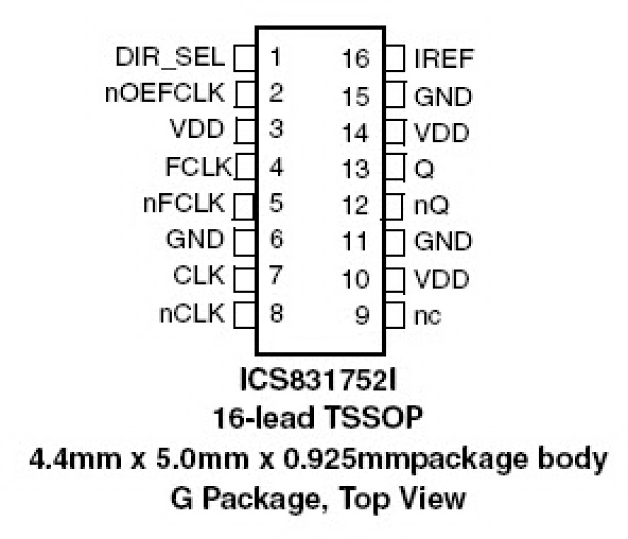
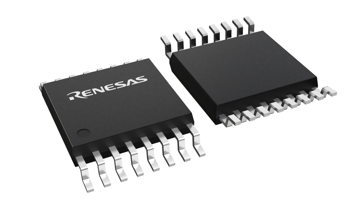
| Pkg. Type: | TSSOP |
| Pkg. Code: | PGG16 |
| Lead Count (#): | 16 |
| Pkg. Dimensions (mm): | 5.0 x 4.4 x 1.0 |
| Pitch (mm): | 0.65 |
环境和出口类别
| Moisture Sensitivity Level (MSL) | 1 |
| Pb (Lead) Free | Yes |
| ECCN (US) | EAR99 |
| HTS (US) | 8542.39.0090 |
产品属性
| Lead Count (#) | 16 |
| Carrier Type | Reel |
| Moisture Sensitivity Level (MSL) | 1 |
| Qty. per Reel (#) | 2500 |
| Qty. per Carrier (#) | 0 |
| Pb (Lead) Free | Yes |
| Pb Free Category | e3 Sn |
| Temp. Range (°C) | -40 to 85°C |
| Additive Phase Jitter Typ RMS (fs) | 300 |
| Additive Phase Jitter Typ RMS (ps) | 0.3 |
| Core Voltage (V) | 2.5V, 3.3V |
| Function | Multiplexer |
| Input Freq (MHz) | 500 |
| Input Type | HCSL, LVDS, LVPECL |
| Inputs (#) | 2 |
| Length (mm) | 5 |
| MOQ | 2500 |
| Output Banks (#) | 1 |
| Output Freq Range (MHz) | 500 |
| Output Type | HCSL |
| Output Voltage (V) | 2.5V, 3.3V |
| Outputs (#) | 1 |
| Package Area (mm²) | 22 |
| Pitch (mm) | 0.65 |
| Pkg. Dimensions (mm) | 5.0 x 4.4 x 1.0 |
| Pkg. Type | TSSOP |
| Product Category | Clock Multiplexers |
| Reel Size (in) | 13 |
| Requires Terms and Conditions | Does not require acceptance of Terms and Conditions |
| Tape & Reel | Yes |
| Thickness (mm) | 1 |
| Width (mm) | 4.4 |
有关 831752I 的资源
描述
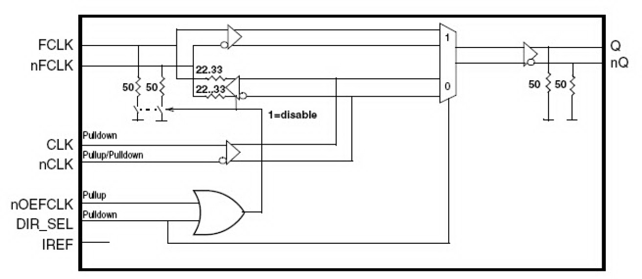
The 831752I is a high-performance, differential HCSL clock switch. The device is designed for the routing of PCIe clock signals in ATCA/AMC system and is optimized for PCIe Gen 1, Gen 2 and Gen 3. The device has one differential, bi-directional I/O (FCLK) for connection to ATCA clock sources and to clock receivers through a connector. The differential clock input CLK is the local clock input and the HCSL output Q is the local clock output. In the common clock mode, FCLK serves as an input and is routed to the differential HCSL output Q. There are two local clock modes. In the local clock mode 0, CLK is the input, Q is the clock output and FCLK is in high-impedance state. In the local clock mode 1, CLK is the input and both Q and FCLK are the outputs of the locally generated PCIe clock signal. The 831752I is characterized to operate from a 3.3V power or 2.5V power supply. The 831752I supports the switching of PCI Express (2.5 Gb/s), Gen 2 (5 Gb/s) and Gen 3 (8 Gb/s) clock signals.


