
特性
- Twelve LVCMOS/LVTTL outputs
- Selectable differential CLK/nCLK or LVCMOS/LVTTL clock input
- CLK/nCLK pair can accept the following differential input levels: LVPECL, LVDS, LVHSTL, SSTL, HCSL
- LVCMOS_CLK supports the following input types: LVCMOS, LVTTL
- Output frequency: 350MHz
- Additive phase jitter, RMS: 0.14ps (typical)
- Output skew: 100ps (maximum), 3.3V±5%
- Part-to-part skew: 1ns (maximum), 3.3V±5%
- Operating supply modes:
Core/Output
3.3V/3.3V
3.3V/2.5V
2.5V/2.5V - -40°C to 85°C ambient operating temperature
- Available in lead-free (RoHS 6) package
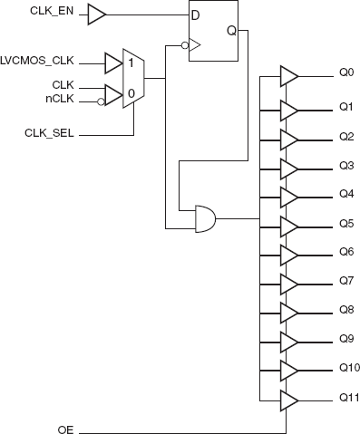
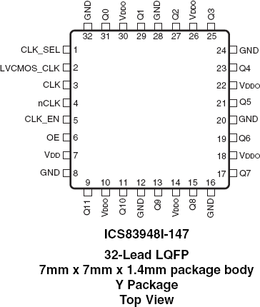
描述
The 83948I-147 is a low skew, 1-to-12 Differential-to-LVCMOS/LVTTL Fanout Buffer. The 83948I-147 has two selectable clock inputs. The CLK, nCLK pair can accept most standard differential input levels. The LVCMOS_CLK can accept LVCMOS or LVTTL input levels. The low impedance LVCMOS/LVTTL outputs are designed to drive 50Ω series or parallel terminated transmission lines. The effective fanout can be increased from 12 to 24 by utilizing the ability of the outputs to drive two series terminated lines. The 83948I-147 is characterized at full 3.3V, full 2.5V or mixed 3.3V core/2.5V output operating supply modes. Guaranteed output and part-to-part skew characteristics make the 83948I-147 ideal for those clock distribution applications demanding well defined performance and repeatability.