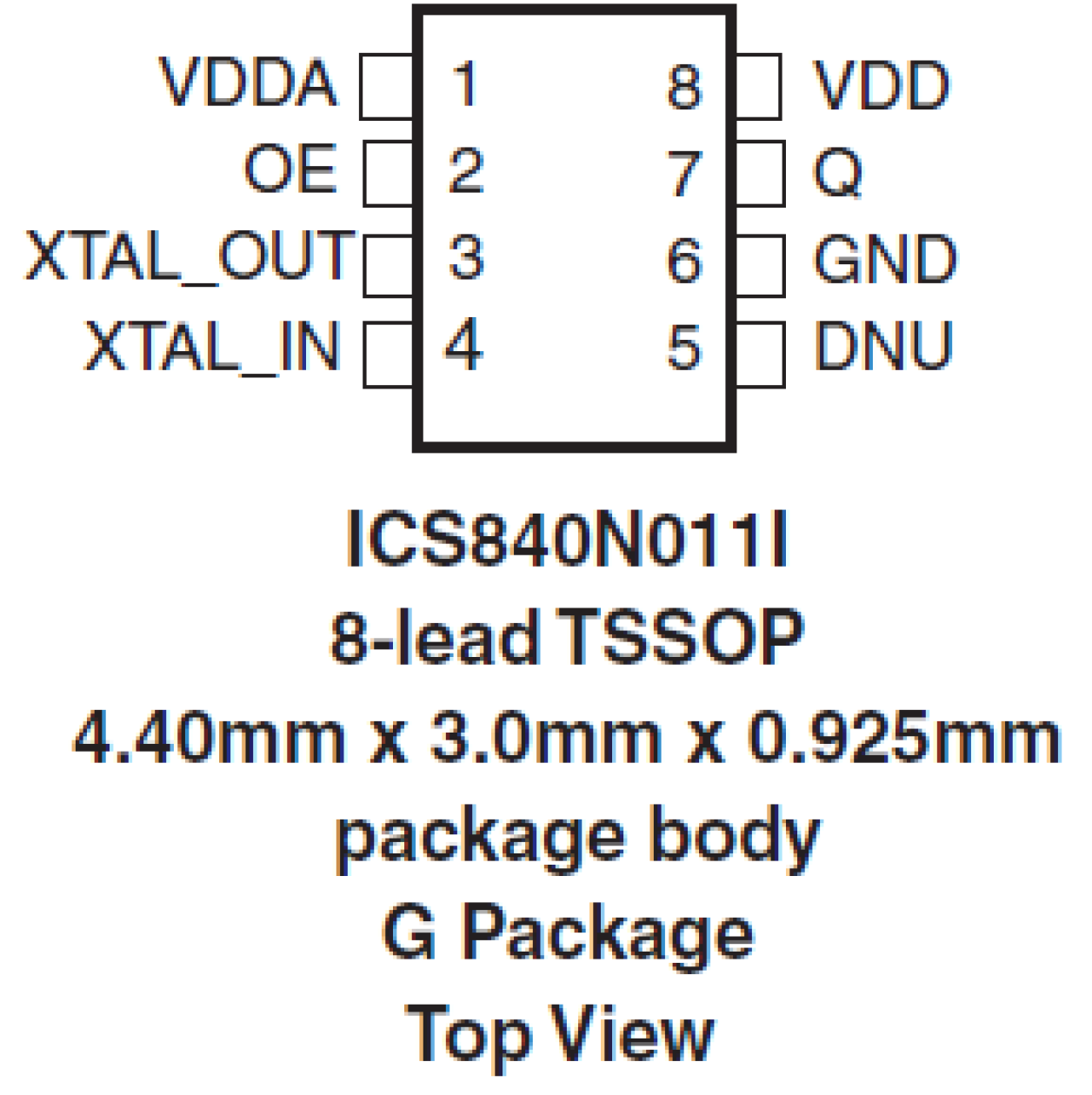
封装信息
| CAD 模型: | View CAD Model |
| Pkg. Type: | TSSOP |
| Pkg. Code: | PGG8 |
| Lead Count (#): | 8 |
| Pkg. Dimensions (mm): | 3.1 x 4.4 x 1.0 |
| Pitch (mm): | 0.65 |
环境和出口类别
| Moisture Sensitivity Level (MSL) | 1 |
| Pb (Lead) Free | Yes |
| ECCN (US) | EAR99 |
| HTS (US) | 8542.39.0090 |
产品属性
| Lead Count (#) | 8 |
| Carrier Type | Tube |
| Moisture Sensitivity Level (MSL) | 1 |
| Qty. per Reel (#) | 0 |
| Qty. per Carrier (#) | 96 |
| Pb (Lead) Free | Yes |
| Pb Free Category | e3 Sn |
| Temp. Range (°C) | -40 to 85°C |
| Core Voltage (V) | 2.5V, 3.3V |
| Feedback Input | No |
| Input Freq (MHz) | 25 - 25, 26.5625 - 26.5625, 30.72 - 30.72, 31.25 - 31.25 |
| Input Type | Crystal |
| Inputs (#) | 1 |
| Length (mm) | 3.1 |
| MOQ | 96 |
| Output Banks (#) | 1 |
| Output Freq Range (MHz) | 106.25 - 106.25, 125 - 125, 122.88 - 122.88, 100 - 100 |
| Output Type | LVCMOS |
| Output Voltage (V) | 2.5V, 3.3V |
| Outputs (#) | 1 |
| Package Area (mm²) | 13.6 |
| Phase Jitter Max RMS (ps) | 0.177 |
| Phase Jitter Typ RMS (ps) | 0.139 |
| Pitch (mm) | 0.65 |
| Pkg. Dimensions (mm) | 3.1 x 4.4 x 1.0 |
| Pkg. Type | TSSOP |
| Product Category | FemtoClock, Ultra-Low Jitter Clocks (<300 fs RMS) |
| Prog. Clock | No |
| Reference Output | No |
| Requires Terms and Conditions | Does not require acceptance of Terms and Conditions |
| Spread Spectrum | No |
| Tape & Reel | No |
| Thickness (mm) | 1 |
| Width (mm) | 4.4 |
| 已发布 | No |
有关 840N011I 的资源
描述
The 840N011I is an LVCMOS/LVTTL clock synthesizer designed for Fibre Channel applications. The device generates a 106.25MHz clock signal from a 26.5625MHz crystal or a 100MHz clock signal from a 25MHz crystal with excellent phase jitter performance. The 840N011I uses Renesas' fourth generation FemtoClock® NG technology for an optimum of high clock frequency, low phase noise performance and low power consumption, and high power supply noise rejection.The device supports 2.5V or 3.3V voltage supply and is packaged in a small, lead-free (RoHS 6) 8-lead TSSOP package. The extended temperature range supports wireless infrastructure, telecommunication, and networking end equipment requirements.

