
特性
- Fourth generation FemtoClock™ (NG) technology
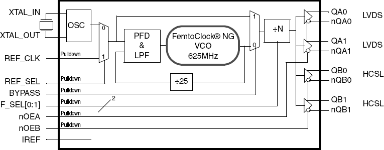
- Selectable 250MHz, 156.25MHz, 125MHz or 100MHz output clock synthesized from a 25MHz fundamental mode crystal
- Four differential clock outputs (two LVDS and two HCSL outputs)
- Crystal interface designed for 25MHz, parallel resonant crystal
- RMS phase jitter at 156.25MHz, using a 25MHz crystal (1MHz - 20MHz): 0.27ps (typical)
- RMS phase jitter at 156.25MHz, using a 25MHz crystal (12kHz - 20MHz): 0.32ps (typical)
- Power supply noise rejection PSNR: -50dB (typical)
- LVCMOS interface levels for the frequency select input
- Full 3.3V or 2.5V supply voltage
- Available in Lead-free (RoHS 6) package
- -40°C to 85°C ambient operating temperature
描述
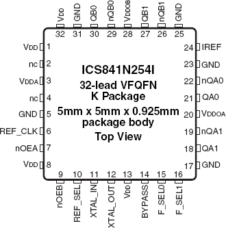
The 841N254I is a 4-output clock synthesizer designed for S-RIO 1.3 and 2.0 reference clock applications. The device generates four copies of a selectable 250MHz, 156.25MHz, 125MHz or 100MHz clock signal with excellent phase jitter performance. The four outputs are organized in two banks of two LVDS and two HCSL outputs. The device uses Renesas' fourth generation FemtoClock™ NG technology for an optimum of high clock frequency and low phase noise performance, combined with a low power consumption and high power supply noise rejection. The synthesized clock frequency and the phase-noise performance are optimized for driving RIO 1.3 and 2.0 SerDes reference clocks. The device supports 3.3V and 2.5V voltage supplies and is packaged in a small 32-lead VFQFN package. The extended temperature range supports wireless infrastructure, telecommunication and networking end equipment requirements.