封装信息
| CAD 模型: | View CAD Model |
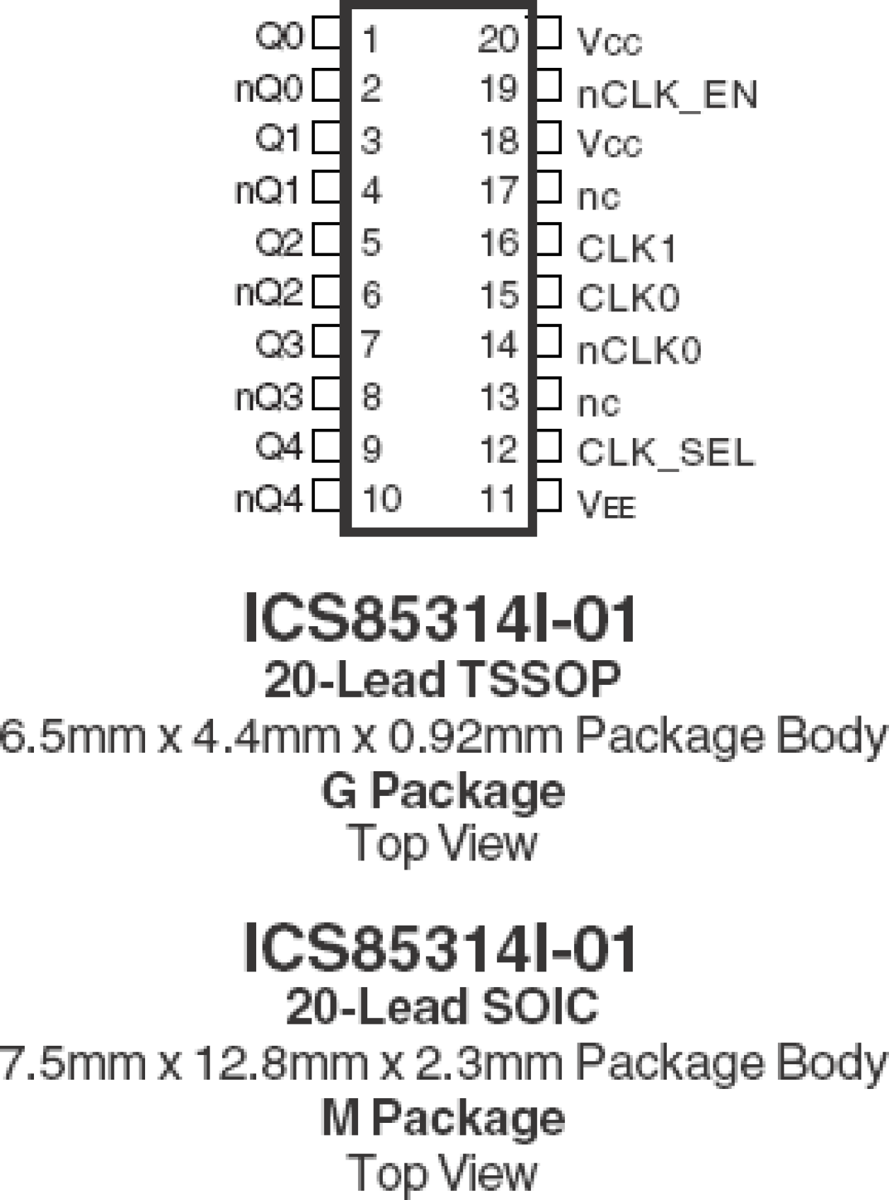
| Pkg. Type: | TSSOP |
| Pkg. Code: | PGG20 |
| Lead Count (#): | 20 |
| Pkg. Dimensions (mm): | 6.5 x 4.4 x 1.0 |
| Pitch (mm): | 0.65 |
环境和出口类别
| Moisture Sensitivity Level (MSL) | 1 |
| Pb (Lead) Free | Yes |
| ECCN (US) | EAR99 |
| HTS (US) | 8542.39.0090 |
产品属性
| Lead Count (#) | 20 |
| Carrier Type | Tube |
| Moisture Sensitivity Level (MSL) | 1 |
| Qty. per Reel (#) | 0 |
| Qty. per Carrier (#) | 74 |
| Output Skew (ps) | 30 |
| Package Area (mm²) | 28.6 |
| Pitch (mm) | 0.65 |
| Pkg. Dimensions (mm) | 6.5 x 4.4 x 1.0 |
| Pb (Lead) Free | Yes |
| Pb Free Category | e3 Sn |
| Temp. Range (°C) | -40 to 85°C |
| Additive Phase Jitter Typ RMS (fs) | 50 |
| Additive Phase Jitter Typ RMS (ps) | 0.05 |
| Core Voltage (V) | 2.5V, 3.3V |
| Function | Buffer, Multiplexer |
| Input Freq (MHz) | 700 |
| Input Type | HCSL, HSTL, LVCMOS, LVDS, LVPECL, SSTL |
| Inputs (#) | 2 |
| Length (mm) | 6.5 |
| MOQ | 148 |
| Output Banks (#) | 1 |
| Output Freq Range (MHz) | 700 |
| Output Type | LVPECL |
| Output Voltage (V) | 2.5V, 3.3V |
| Outputs (#) | 5 |
| Pkg. Type | TSSOP |
| Price (USD) | $6.25946 |
| Product Category | Clock Buffers & Drivers, Clock Multiplexers |
| Requires Terms and Conditions | Does not require acceptance of Terms and Conditions |
| Tape & Reel | No |
| Thickness (mm) | 1 |
| Width (mm) | 4.4 |
| 已发布 | No |
有关 85314I-01 的资源
描述
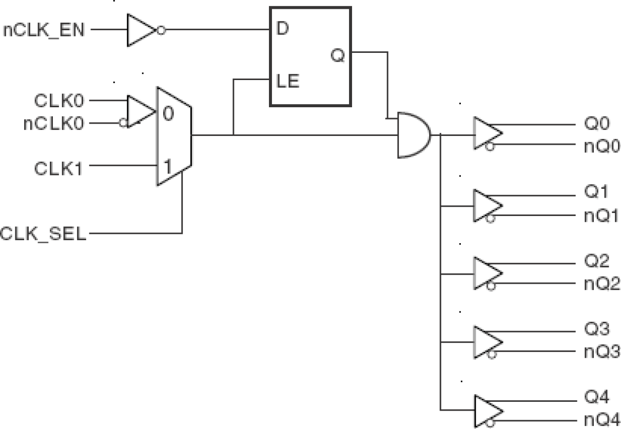
The 85314I-01 is a low skew, high performance 1-to-5 Differential-to-2.5V/3.3V LVPECL Fanout Buffer.The 85314I-01 has two selectable clock inputs. The CLK0, nCLK0 pair can accept most standarddifferential input levels. The single-ended CLK1 can accept LVCMOS or LVTTL input levels. The clock enable is internally synchronized to eliminate runt clock pulses on the outputs during asynchronous assertion/deassertion of the clockenable pin. Guaranteed output and part-to-part skew characteristics make the 85314I-01 ideal for those applications demanding well defined performance and repeatability.

