
特性
- Four differential LVDS output pairs
- Selectable differential CLK, nCLK or LVPECL clock inputs
- CLK, nCLK pair can accept the following differential input levels: LVPECL, LVDS, LVHSTL, SSTL, HCSL
- PCLK, nPCLK pair supports the following input types: LVPECL, CML, SSTL
- Maximum output frequency: 800MHz
- Translates any single-ended input signal to LVDS levels with resistor bias on nCLK input
- Additive phase jitter, RMS: 0.146ps (typical)
- Output skew: 100ps (maximum)
- Part-to-Part skew: 700ps (maximum)
- Propagation delay: 3.3ns (maximum)
- Full 3.3V supply mode
- 0 °C to 70 °C ambient operating temperature
- Available in a lead-free (RoHS 6) package
- Industrial temperature information available upon request
描述
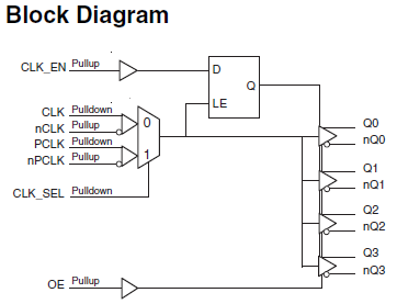
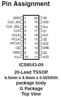
The ICS8543-09 is a low-skew, high-performance 1-to-4 differential-to-LVDS clock fanout buffer. Utilizing Low Voltage Differential Signaling (LVDS) the ICS8543-09 provides a low power, low noise, solution for distributing clock signals over controlled impedances of 100Ω. The device has two selectable clock inputs. The CLK, nCLK pair can accept most standard differential input levels. The PCLK, nPCLK pair can accept LVPECL, CML, or SSTL input levels. The clock enable is internally synchronized to eliminate runt pulses on the outputs during asynchronous assertion/de-assertion of the clock enable pin.
Guaranteed output and part-to-part skew characteristics make the ICS8543-09 ideal for those applications demanding well-defined performance and repeatability.


