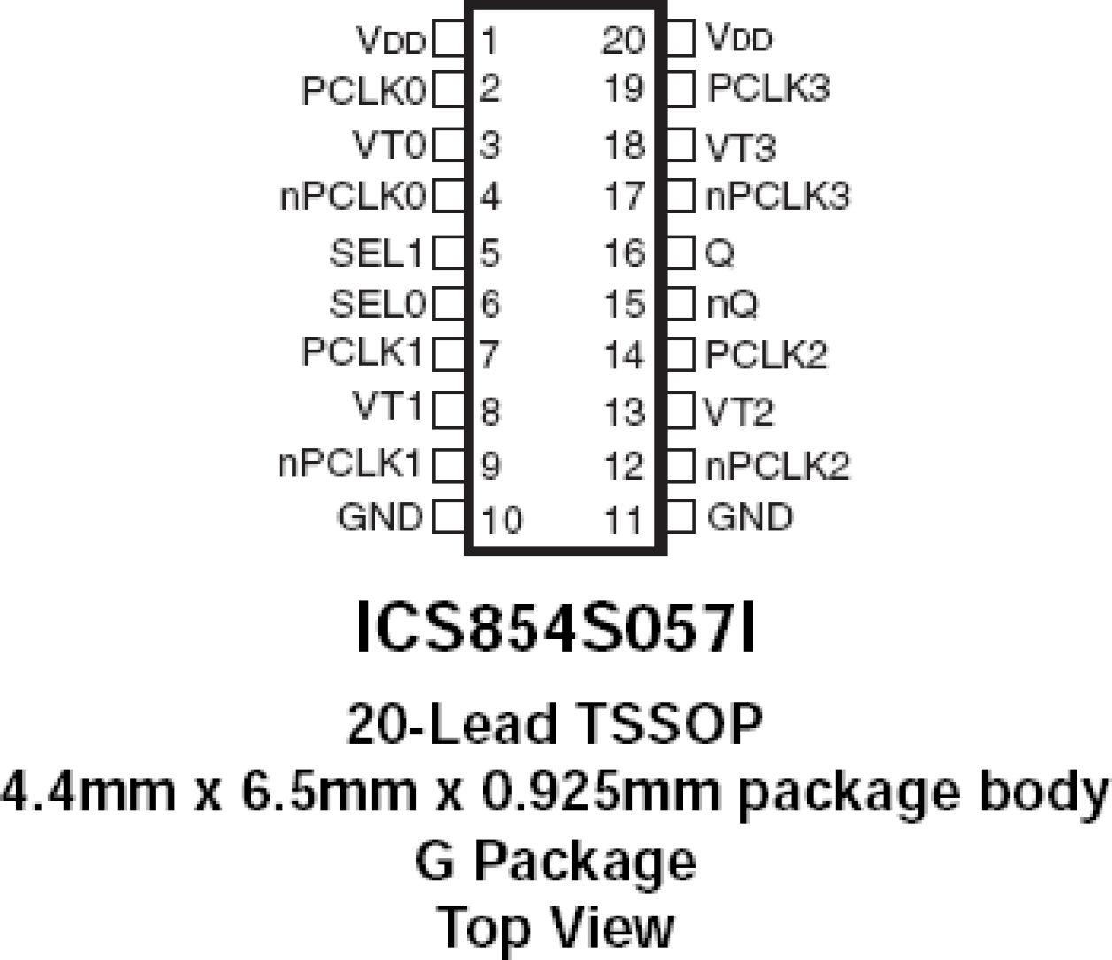
封装信息
| CAD 模型: | View CAD Model |
| Pkg. Type: | TSSOP |
| Pkg. Code: | PGG20 |
| Lead Count (#): | 20 |
| Pkg. Dimensions (mm): | 6.5 x 4.4 x 1.0 |
| Pitch (mm): | 0.65 |
环境和出口类别
| Moisture Sensitivity Level (MSL) | 1 |
| Pb (Lead) Free | Yes |
| ECCN (US) | EAR99 |
| HTS (US) | 8542.39.0090 |
产品属性
| Lead Count (#) | 20 |
| Carrier Type | Reel |
| Moisture Sensitivity Level (MSL) | 1 |
| Qty. per Reel (#) | 3000 |
| Qty. per Carrier (#) | 0 |
| Pb (Lead) Free | Yes |
| Pb Free Category | e3 Sn |
| Temp. Range (°C) | -40 to 85°C |
| Additive Phase Jitter Typ RMS (fs) | 47 |
| Additive Phase Jitter Typ RMS (ps) | 0.047 |
| Core Voltage (V) | 2.5 |
| Function | Multiplexer |
| Input Freq (MHz) | 2000 |
| Input Type | CML, LVDS, LVPECL, SSTL |
| Inputs (#) | 4 |
| Length (mm) | 6.5 |
| MOQ | 3000 |
| Output Banks (#) | 1 |
| Output Freq Range (MHz) | 2000 |
| Output Type | LVDS |
| Output Voltage (V) | 2.5 |
| Outputs (#) | 1 |
| Package Area (mm²) | 28.6 |
| Pitch (mm) | 0.65 |
| Pkg. Dimensions (mm) | 6.5 x 4.4 x 1.0 |
| Pkg. Type | TSSOP |
| Product Category | Clock Multiplexers |
| Reel Size (in) | 13 |
| Requires Terms and Conditions | Does not require acceptance of Terms and Conditions |
| Tape & Reel | Yes |
| Thickness (mm) | 1 |
| Width (mm) | 4.4 |
有关 854S057I 的资源
描述
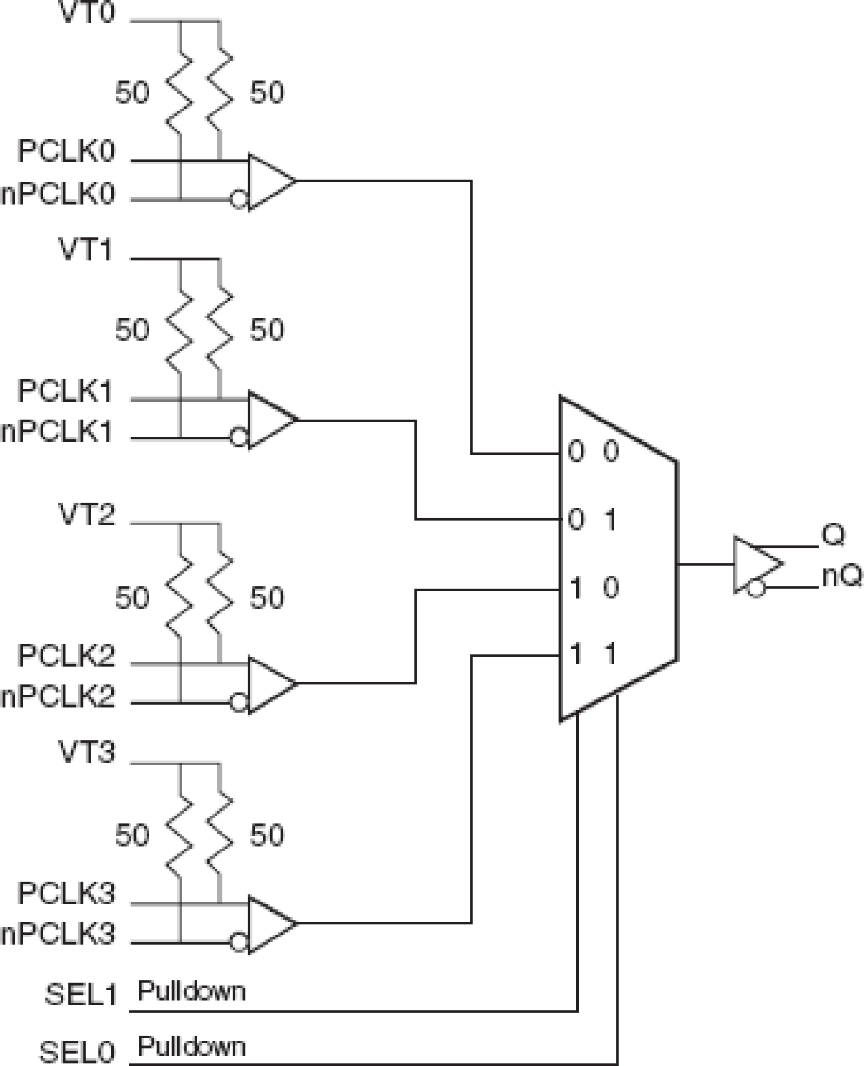
The 854S057I is a 4:1 or 2:1 LVDS Clock Multiplexer which can operate up to 2GHz. The PCLK, nPCLK pairs can accept most standard differential input levels. Internal termination is provided on each differential input pair. The 854S057I operates using a 2.5V supply voltage. The fully differential architecture and low propagation delay make it ideal for use in high speed multiplexing applications. The select pins have internal pulldown resistors. Leaving one input unconnected (pulled to logic low by the internal resistor) will transform the device into a 2:1 multiplexer. The SEL1 pin is the most significant bit and the binary number applied to the select pins will select the same numbered data input (i.e., 00 selects PCLK0, nPCLK0).

