封装信息
| CAD 模型: | View CAD Model |
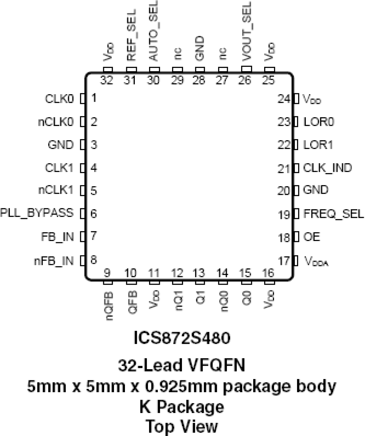
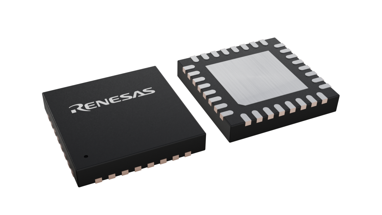
| Pkg. Type: | VFQFPN |
| Pkg. Code: | NLG32 |
| Lead Count (#): | 32 |
| Pkg. Dimensions (mm): | 5.0 x 5.0 x 0.9 |
| Pitch (mm): | 0.5 |
环境和出口类别
| Moisture Sensitivity Level (MSL) | 3 |
| Pb (Lead) Free | Yes |
| ECCN (US) | EAR99 |
| HTS (US) | 8542.39.0090 |
产品属性
| Lead Count (#) | 32 |
| Carrier Type | Tray |
| Moisture Sensitivity Level (MSL) | 3 |
| Qty. per Reel (#) | 0 |
| Qty. per Carrier (#) | 490 |
| Pb (Lead) Free | Yes |
| Pb Free Category | e3 Sn |
| Temp. Range (°C) | 0 to 70°C |
| Advanced Features | Feedback Input |
| C-C Jitter Max P-P (ps) | 25 |
| Core Voltage (V) | 3.3 |
| Feedback Input | Yes |
| Input Freq (MHz) | 350 - 950 |
| Input Type | HCSL, HSTL, LVDS, LVPECL |
| Inputs (#) | 2 |
| Length (mm) | 5 |
| MOQ | 490 |
| Output Banks (#) | 1 |
| Output Freq Range (MHz) | 350 - 950 |
| Output Skew (ps) | 20 |
| Output Type | HSTL |
| Output Voltage (V) | 3.3 |
| Outputs (#) | 2 |
| Package Area (mm²) | 25 |
| Pitch (mm) | 0.5 |
| Pkg. Dimensions (mm) | 5.0 x 5.0 x 0.9 |
| Pkg. Type | VFQFPN |
| Product Category | Zero Delay Buffers |
| Prog. Clock | No |
| Requires Terms and Conditions | Does not require acceptance of Terms and Conditions |
| Tape & Reel | No |
| Thickness (mm) | 0.9 |
| Width (mm) | 5 |
有关 872S480 的资源
描述
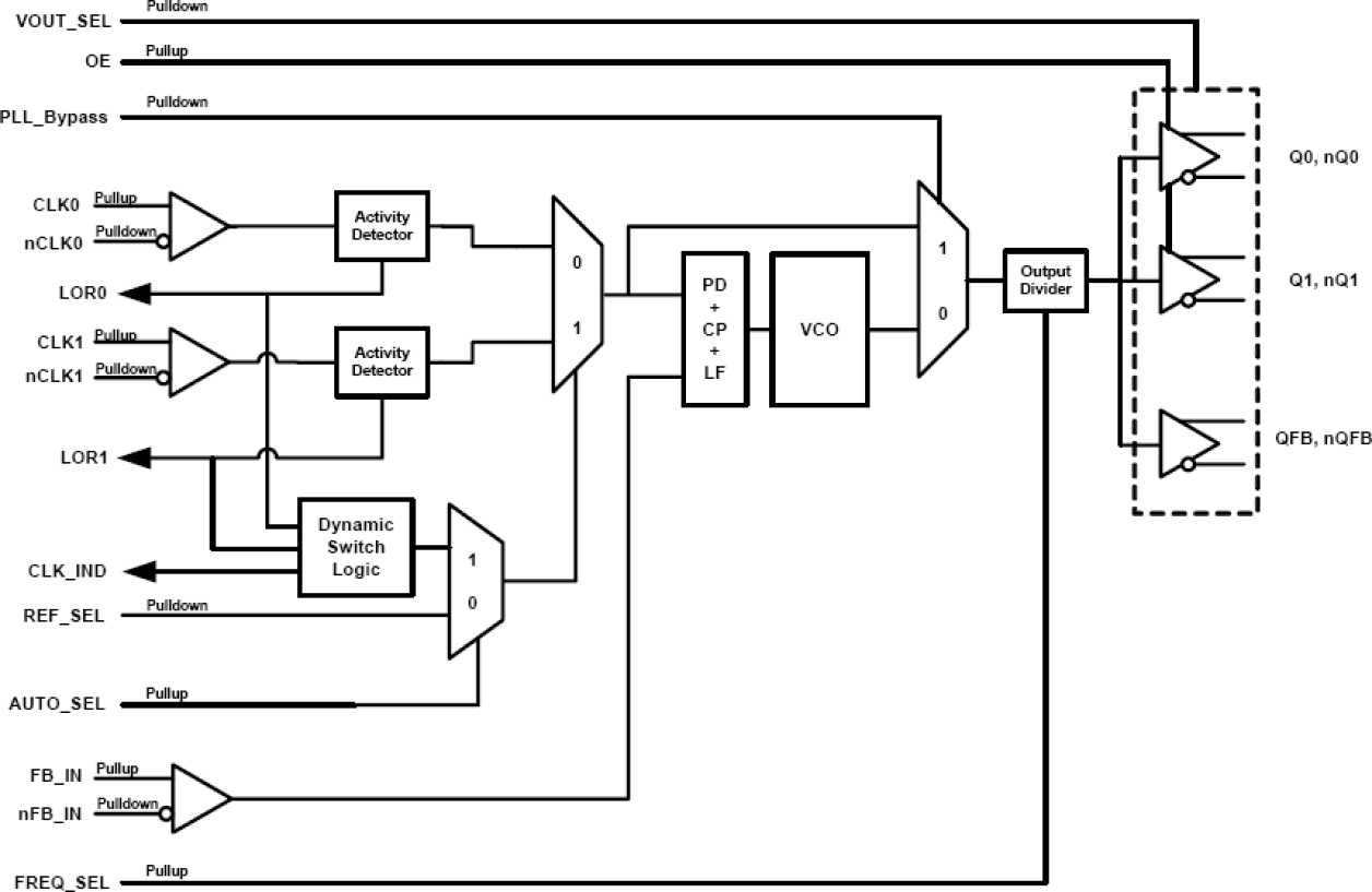
The 872S480 is a Zero Delay Clock Generator with hitless input clock switching capability. The 872S480 is ideal for use in redundant, fault tolerant clock trees where low jitter frequency synthesis are critical. The device receives two differential clock signals from which it generates two outputs with "zero" delay. The output and feedback dividers are configured to allow for a 1:1 frequency generation ratio. The 872S480 Dynamic Clock Switch (DCS) circuit continuously monitors both input clock signals. Upon detection of an invalid clock input (stuck LOW or HIGH for at least one complete clock period of the VCO feedback frequency), the loss of reference monitor will be set HIGH. If that clock is the primary clock, the DCS will switch to the good secondary clock and phase/frequency alignment will occur with minimal output phase disturbance. Once the primary clock is restored to a good state, the DCS will automatically switch back to the primary clock input. The low jitter characteristics with input clock monitoring and DCS capability make the 872S480 an ideal choice for DDR3 applications requiring fault tolerant reference clocks.


