
| CAD 模型: | View CAD Model |
| Pkg. Type: | VFQFPN |
| Pkg. Code: | NLG16 |
| Lead Count (#): | 16 |
| Pkg. Dimensions (mm): | 3.0 x 3.0 x 1.0 |
| Pitch (mm): | 0.5 |
| Moisture Sensitivity Level (MSL) | 3 |
| Pb (Lead) Free | Yes |
| ECCN (US) | EAR99 |
| HTS (US) | 8542.39.0090 |
| Lead Count (#) | 16 |
| Carrier Type | Reel |
| Moisture Sensitivity Level (MSL) | 3 |
| Qty. per Reel (#) | 2500 |
| Qty. per Carrier (#) | 0 |
| Pb (Lead) Free | Yes |
| Pb Free Category | e3 Sn |
| Temp. Range (°C) | -40 to 85°C |
| Additive Phase Jitter Typ RMS (fs) | 57 |
| Additive Phase Jitter Typ RMS (ps) | 0.057 |
| Adjustable Phase | No |
| Advanced Features | Per-bank divider |
| Channels (#) | 1 |
| Core Voltage (V) | 2.5V, 3.3V |
| Divider Value | 1, 2, 4, 8 |
| Function | Buffer, Divider |
| Input Freq (MHz) | 1000 |
| Input Type | LVPECL, LVDS, CML |
| Inputs (#) | 1 |
| Length (mm) | 3 |
| MOQ | 2500 |
| Noise Floor (dBc/Hz) | -154 |
| Output Banks (#) | 2 |
| Output Freq Range (MHz) | 1000, 200 |
| Output Type | LVPECL, LVCMOS |
| Output Voltage (V) | 2.5V, 3.3V |
| Outputs (#) | 2 |
| Package Area (mm²) | 9 |
| Pitch (mm) | 0.5 |
| Pkg. Dimensions (mm) | 3.0 x 3.0 x 1.0 |
| Pkg. Type | VFQFPN |
| Product Category | Clock Buffers & Drivers, Clock Dividers, RF Buffers |
| Reel Size (in) | 13 |
| Requires Terms and Conditions | Does not require acceptance of Terms and Conditions |
| Supply Voltage (V) | 2.5 - 2.5, 3.3 - 3.3 |
| Tape & Reel | Yes |
| Thickness (mm) | 1 |
| Width (mm) | 3 |
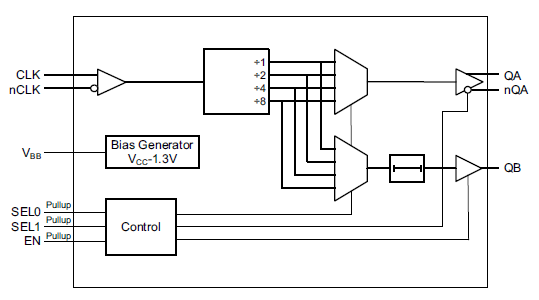
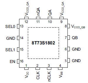
The 8T73S1802 is a fully integrated clock fanout buffer and frequency divider. The input signal is frequency-divided and then fanned out to one differential LVPECL and one LVCMOS output. Each of the outputs can select its individual divider value from the range of ÷1, ÷2, ÷4 and ÷8. Three control inputs EN, SEL0, and SEL1 (3-level logic) are available to select the frequency dividers and the output enable/disable state. The single-ended LVCMOS output is phase-delayed by 650ps to minimize coupling of LVCMOS switching into the differential output during its signal transition.
The 8T73S1802 is optimized to deliver very low phase noise clocks. The VBB output generates a common-mode voltage reference for the differential clock input so that connecting the VBB pin to an unused input (nCLK) enables to use of single-ended input signals. The extended temperature range supports wireless infrastructure, telecommunication, and networking end equipment requirements. The 8T73S1802 can be used with a 3.3V or a 2.5V power supply.