
特性
- Four banks of two output pairs
- Individual output type control, LVDS or LVPECL, via serial interface
- Individual outputs remain enabled while serial loading new device configurations
- One differential PCLK, nPCLK input
- PCLK, nPCLK input pair can accept the following differential input levels: LVPECL, LVDS levels
- Maximum input frequency: 1.5GHz
- LVCMOS control inputs
- Individual output enable/disable control via serial interface
- 2.375V to 3.465V supply voltage operation
- -40°C to 85°C ambient operating temperature
- Lead-free (RoHS 6) packaging
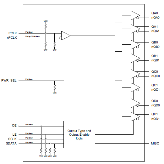
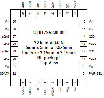
8T79S838-08I - Block Diagram
描述
The IDT8T79S838-08I is a high performance, 1-to-8, differential input to universal output fanout buffer. The device is designed for signal fanout of high-frequency clock signals in applications requiring output frequencies generated simultaneously. The IDT8T79S838-08I is optimized for 3.3V and 2.5V supply voltages and a temperature range of -40°C to 85°C. The device is packaged in a space-saving 32 lead VFQFN package.


