特性
- High-performance clock RF sampling clock generator and clock jitter attenuator with support for JESD204B/C
- Low phase noise: -144.7dBc/Hz (800kHz offset; 491.52MHz)
- Integrated phase noise of 74fs RMS (12kHz–20MHz, 491.52MHz)
- Dual-PLL architecture with internal and optional external VCO
- Eight output channels with a total of 18 outputs
- Configurable integer clock frequency dividers
- Clock output frequencies: up to 3932.16MHz (internal VCO) and 6GHz (optional external VCO)
- Differential, low noise I/O
- Deterministic phase delay and integrated phase delay circuits
- Redundant input clock architecture with four inputs and monitors, holdover and input switching
- SPI 3/4 wire configuration interface
- Supply voltage: 1.8V (core, outputs) and 3.3V (high performance outputs)
- Package: 100-CABGA (11 × 11 mm²)
- Temperature range: -40°C to +95°C (board)


描述
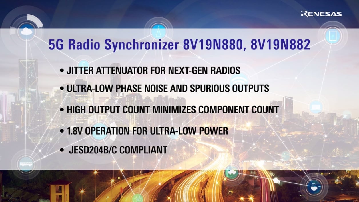
The 8V19N880 is a fully integrated FemtoClock® RF Sampling Clock Generator and Jitter Attenuator designed as a high-performance clock solution for conditioning and frequency/phase management of wireless base station radio equipment boards. The device is optimized to deliver excellent phase noise performance as required in 4G, 5G and including mmWave radio implementations. The device supports JESD204B (subclass 0 and 1) and JESD204C.
A two-stage PLL architecture supports both jitter attenuation and frequency multiplication. The first stage PLL is the jitter attenuator and uses an external VCXO for the best possible phase noise characteristics. The second stage PLL locks on the first PLL output signal and synthesizes the target frequency. The second stage PLL can use the internal or an external high-frequency VCO.
The device generates the high-frequency clocks and the low-frequency synchronization signals (SYSREF) from the selected VCO. SYSREF signals are internally synchronized to the clock signals. The integrated signal delay blocks can be used to achieve phase alignment, controlled phase offsets between system reference and clock signals and to align/delay individual output signals. The four redundant inputs are monitored for activity. Four selectable clock switching modes are provided to handle clock input failure scenarios. Auto-lock, individually programmable output frequency dividers, and phase adjustment capabilities are added for flexibility.
The device is configured through a 3/4-wire SPI interface and reports lock and signal loss status in internal registers and via the GPIO[1:0] outputs. Internal status bit changes can also be reported via a GPIO output.
For information regarding evaluation boards and material, please contact your local sales representative.
The 8V19N880 and 8V19N882 JESD204B/C clock jitter attenuators deliver low phase noise and exceptional jitter performance as low as 74fs RMS and -90dB spurious attenuation for mission-critical industrial data converter applications in wireless radio, test and measurement, instrumentation, and high-performance imaging. They support frequencies up to 3932.16MHz (up to 6GHz with an external VCO) and feature 16 and 18 integrated differential outputs to deliver a first-in-class balance of high performance, low voltage and low power consumption with 1.8V support.
活动与在线研讨会

新闻和博客
博客
2022年2月1日
|
新闻
2021年11月10日
|
