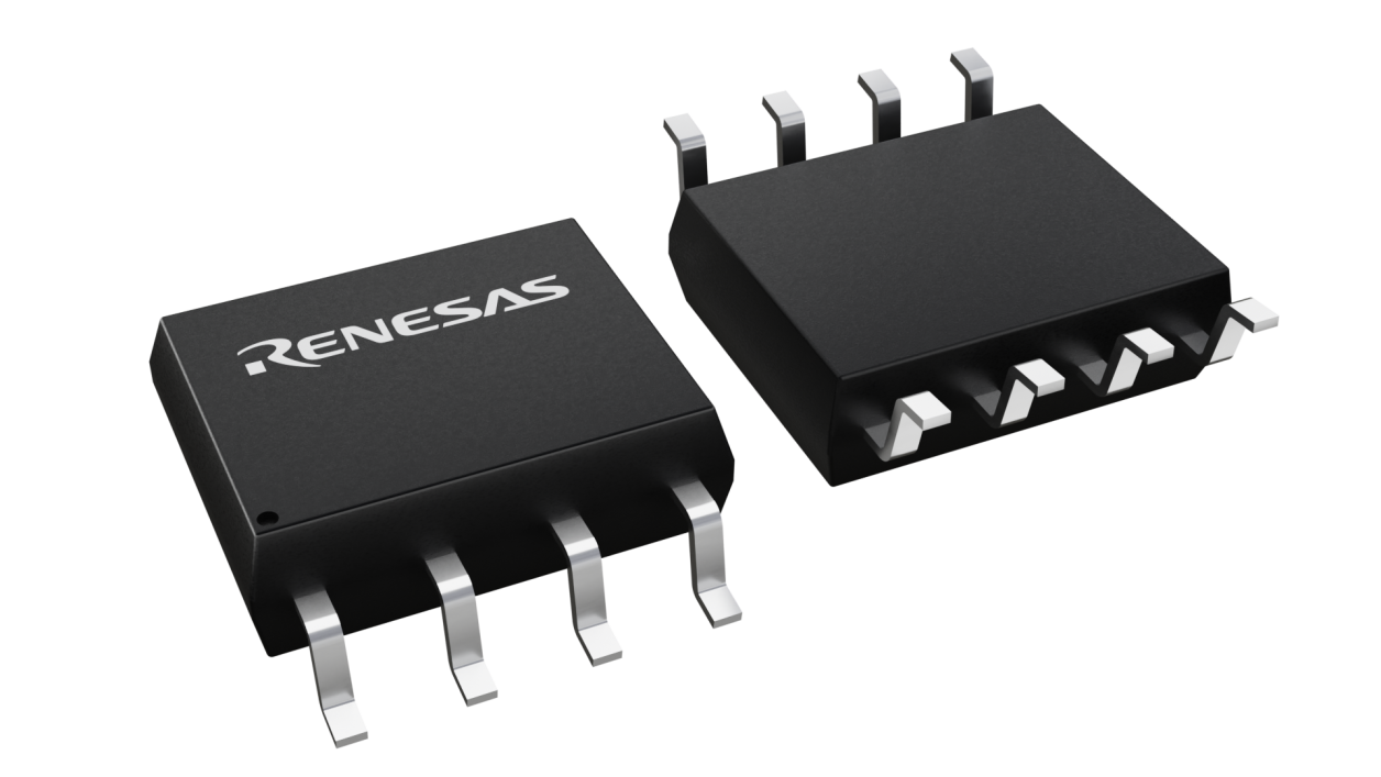
封装信息
| CAD 模型: | View CAD Model |
| Pkg. Type: | SOIC |
| Pkg. Code: | DCG8 |
| Lead Count (#): | 8 |
| Pkg. Dimensions (mm): | 4.9 x 3.9 x 1.5 |
| Pitch (mm): | 1.27 |
环境和出口类别
| Moisture Sensitivity Level (MSL) | 1 |
| Pb (Lead) Free | Yes |
| ECCN (US) | EAR99 |
| HTS (US) | 8542.39.0090 |
产品属性
| Lead Count (#) | 8 |
| Carrier Type | Reel |
| Moisture Sensitivity Level (MSL) | 1 |
| Qty. per Reel (#) | 3000 |
| Qty. per Carrier (#) | 0 |
| Package Area (mm²) | 19.1 |
| Pitch (mm) | 1.27 |
| Pkg. Dimensions (mm) | 4.9 x 3.9 x 1.5 |
| Pb (Lead) Free | Yes |
| Pb Free Category | e3 Sn |
| Temp. Range (°C) | -40 to 85°C |
| Accepts Spread Spec Input | Yes |
| Advanced Features | Accepts Spread Spec Input |
| C-C Jitter Max P-P (ps) | 200 |
| Core Voltage (V) | 3.3 |
| Input Freq (MHz) | 10 - 133 |
| Input Type | LVCMOS |
| Inputs (#) | 1 |
| Length (mm) | 4.9 |
| MOQ | 3000 |
| Output Banks (#) | 1 |
| Output Freq Range (MHz) | 10 - 133 |
| Output Skew (ps) | 250 |
| Output Type | LVCMOS |
| Output Voltage (V) | 3.3 |
| Outputs (#) | 5 |
| Pkg. Type | SOIC |
| Product Category | Zero Delay Buffers |
| Reel Size (in) | 13 |
| Requires Terms and Conditions | Does not require acceptance of Terms and Conditions |
| Supply Voltage (V) | 3.3 - 3.3 |
| Tape & Reel | Yes |
| Thickness (mm) | 1.5 |
| Width (mm) | 3.9 |
有关 91305 的资源
描述
The IDT91305 is a high performance, low skew, low jitter clock driver. It uses a phase lock loop (PLL) technology to align, in both phase and frequency, the REF input with the CLKOUT signal. It is designed to distribute high speed clocks in communication systems operating at speeds from 10 to 133 MHz.
IDT91305 is a zero delay buffer that provides synchronization between the input and output. The synchronization is established via CLKOUT feed back to the input of the PLL. Since the skew between the input and output is less than +/- 350 pS, the part acts as a zero delay buffer.
The IDT91305 comes in an eight pin 150 mil SOIC package. It has five output clocks. In the absence of REF input, will be in the power down mode. In this mode, the PLL is turned off and the output buffers are pulled low. Power down mode provides the lowest power consumption for a standby condition.
