
特性
- 400 - 500 MHz clock source
- 4 open-drain differential output drives with short term jitter < 40ps
- Spread spectrum compatible
- Reference clock is differential or single-ended, 100 or 133 MHz
- SMBus programmability for: - frequency multiplier - output enable - operating mode
- Supports frequency multipliers of: 3, 4, 5, 6, 8, 9/2, 15/2 and 15/4
- Support systems where XDR subsystem is asynchronous to other system clocks
- 2.5V power supply
描述
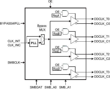
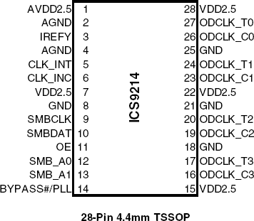
The 9214 clock generator provides the necessary clock signals to support the Rambus XDRTM memory subsystem and Redwood logic interface. The clock source is a reference clock that may or may not be modulated for spread spectrum. The 9214 provides 4 differential clock pairs in a space saving 28-pin TSSOP package and provides an off-the-shelf high-performance interface solution. Figure 1 shows the major components of the 9214 XDR Clock Generator. These include the a PLL, a Bypass Multiplexer and four differential output buffers. The outputs can be disabled by a logic low on the OE pin. An output is enabled by the combination of the OE pin being high, and 1 in its SMBus Output control register bit. The PLL receives a reference clock, CLK_INT/C and outputs a clock signal at a frequency equal to the input frequency times a multiplier. Table 2 shows the multipliers selectable via the SMBus interface. This clock signal is then fed to the differential output buffers to drive the enabled clocks. Disabled outputs are set to Hi-Z. The Bypass mode routes the input clock, CLK_INT/C, directly to the differential output buffers, bypassing the PLL. Up to four 9214 devices can be cascaded on the same SMBus. Table 3 shows the SMBus addressing and control for the four devices.