封装信息
| CAD 模型: | View CAD Model |
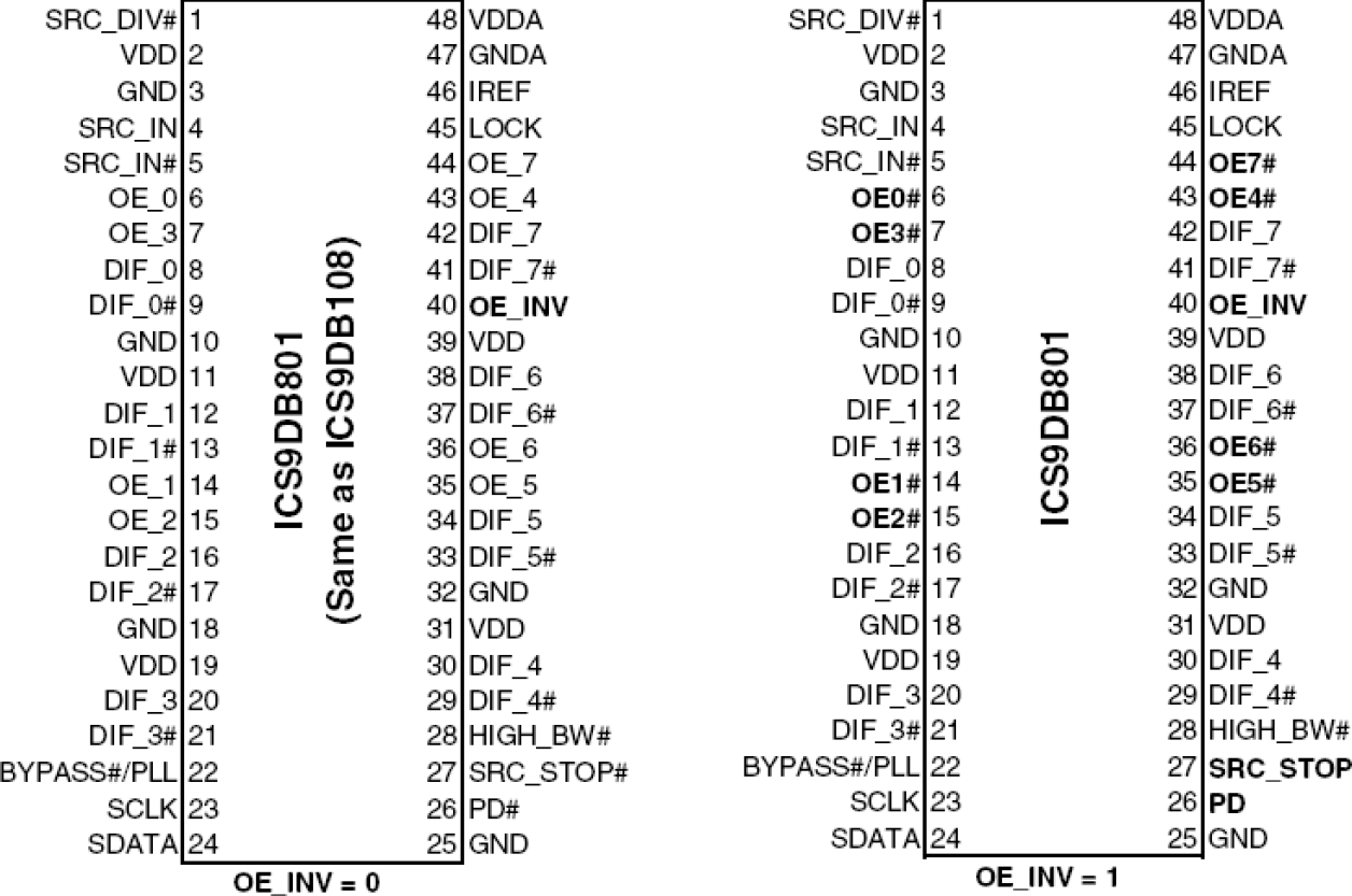
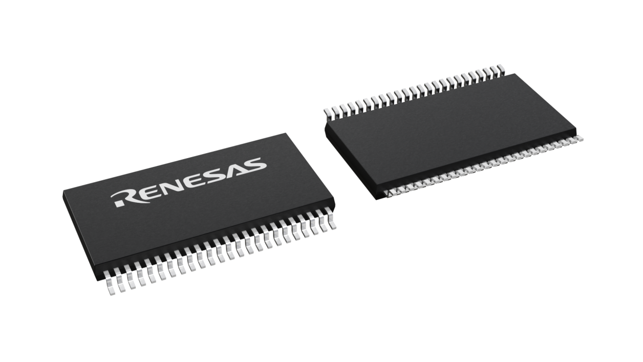
| Pkg. Type: | TSSOP |
| Pkg. Code: | PAG48 |
| Lead Count (#): | 48 |
| Pkg. Dimensions (mm): | 12.5 x 6.1 x 1.0 |
| Pitch (mm): | 0.5 |
环境和出口类别
| Moisture Sensitivity Level (MSL) | 1 |
| Pb (Lead) Free | Yes |
| ECCN (US) | EAR99 |
| HTS (US) | 8542.39.0090 |
产品属性
| Lead Count (#) | 48 |
| Carrier Type | Reel |
| Moisture Sensitivity Level (MSL) | 1 |
| Qty. per Reel (#) | 2000 |
| Qty. per Carrier (#) | 0 |
| Chipset Name | Blackford, Clarksboro, Greencreek, Lindenhurst, Twincastle |
| Input Freq (MHz) | 100 - 200 |
| Package Area (mm²) | 76.3 |
| Pitch (mm) | 0.5 |
| Pkg. Dimensions (mm) | 12.5 x 6.1 x 1.0 |
| Pb (Lead) Free | Yes |
| Pb Free Category | e3 Sn |
| Temp. Range (°C) | 0 to 70°C |
| Accepts Spread Spec Input | Yes |
| Advanced Features | HW PLL mode control |
| App Jitter Compliance | PCIe Gen1 |
| Architecture | Common |
| C-C Jitter Max P-P (ps) | 50 |
| C-C Jitter Typ P-P (ps) | 35 |
| Chipset Manufacturer | Intel |
| Clock Spec. | DB800 |
| Core Voltage (V) | 3.3 |
| Diff. Input Signaling | HCSL |
| Diff. Inputs | 1 |
| Diff. Output Signaling | HCSL |
| Diff. Outputs | 8 |
| Diff. Termination Resistors | 32 |
| Feedback Input | No |
| Input Type | HCSL |
| Inputs (#) | 1 |
| Length (mm) | 12.5 |
| MOQ | 2000 |
| Multiplication Value | 1 |
| Multiply/Divide Value | 2 |
| Output Banks (#) | 1 |
| Output Freq Range (MHz) | 10 - 400 |
| Output Skew (ps) | 50 |
| Output Type | HCSL |
| Output Voltage (V) | 0.8 |
| Outputs (#) | 8 |
| PLL | Yes |
| Pkg. Type | TSSOP |
| Platform Name | Bensley, Caneland, Glidewell, Lindenhurst, Truland |
| Power Consumption Typ (mW) | 533 |
| Product Category | PCI Express Clocks |
| Prog. Clock | No |
| Reel Size (in) | 13 |
| Requires Terms and Conditions | Does not require acceptance of Terms and Conditions |
| Supply Voltage (V) | 3.3 - 3.3 |
| Tape & Reel | Yes |
| Thickness (mm) | 1 |
| Width (mm) | 6.1 |
有关 9DB801 的资源
描述
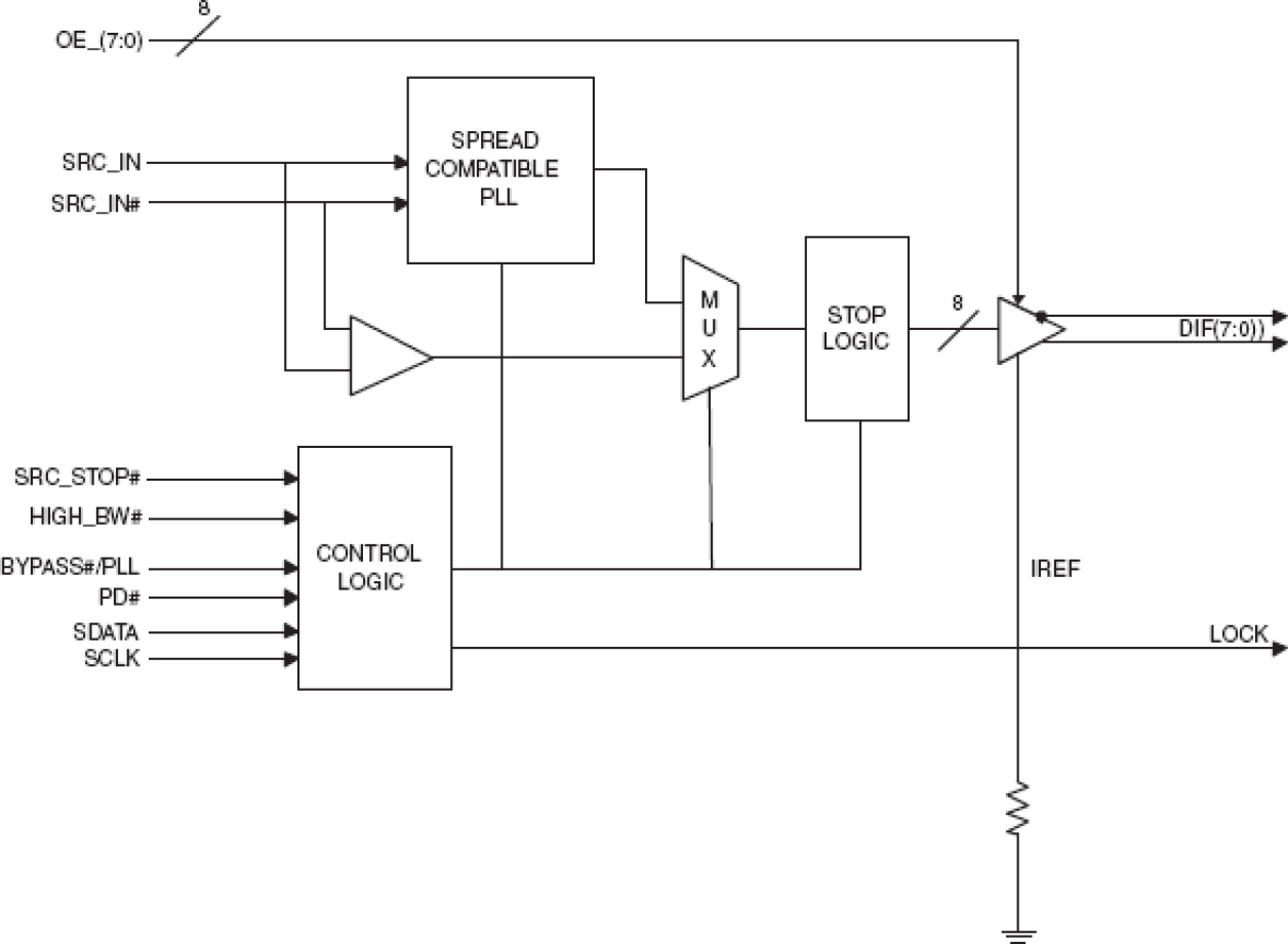
The 9DB801C is a DB800 Version 2.0 Yellow Cover part with PCI Express® support. It can be used in PC or embedded systems to provide outputs that have low cycle-to-cycle jitter (50 ps), low output-to-output skew (100 ps), and are PCI Express® gen 1 compliant. The 9DB801C supports a 1 to 8 output configuration, taking a spread or non spread differential HCSL input from a CK410(B) main clock such as 954101 and 932S401, or any other differential HCSL pair. 9DB801C can generate HCSL or LVDS outputs from 50 to 200 MHz in PLL mode or 0 to 400 MHz in bypass mode. There are two de-jittering modes available selectable through the HIGH_BW# input pin, high bandwidth mode provides de-jittering for spread inputs and low bandwidth mode provides extra de-jittering for non-spread inputs. The SRC_STOP#, PD#, and individual OE# real-time input pins provide completely programmable power management control.


