特性
- LP-HCSL outputs; save 8 resistors compared to standard PCIe devices
- 39 mW typical power consumption; reduced thermal concerns
- OE# pins; support DIF power management
- Programmable slew rate for each output; allows tuning for various line lengths
- Programmable output amplitude; allows tuning for various application environments
- DIF outputs blocked until PLL is locked; clean system start-up
- Selectable 0%, -0.25% or -0.5% spread on DIF outputs; reduces EMI
- External 25 MHz crystal; supports tight ppm with 0 ppm synthesis error
- Configuration can be accomplished with strapping pins; SMBus interface not required for device control
- 3.3 V tolerant SMBus interface works with legacy controllers
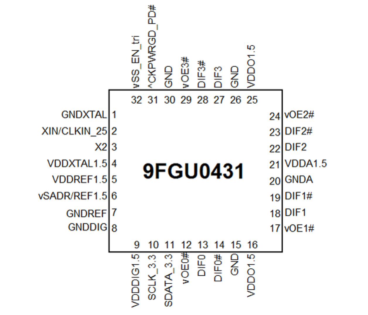
- Space saving 5x5 mm 32-pin VFQFPN; minimal board space
- Selectable SMBus addresses; multiple devices can easily share an SMBus segment
描述
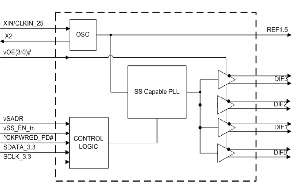
The 9FGU0431 is a member of IDT's 1.5 V Ultra-Low-Power PCIe clock family. The device has 4 output enables for clock management, 2 different spread spectrum levels in addition to spread off, and 2 selectable SMBus addresses.
产品参数
| 属性 | 值 |
|---|---|
| Diff. Outputs | 4 |
| Diff. Output Signaling | LP-HCSL |
| Output Freq Range (MHz) | 25 - 25, 100 - 100 |
| Power Consumption Typ (mW) | 39 |
| Supply Voltage (V) | 1.5 - 1.5 |
| Output Type | LP-HCSL, LVCMOS |
| Xtal Freq (MHz) | 25 - 25 |
| Diff. Termination Resistors | 8 |
| Package Area (mm²) | 25 |
| Battery Backup | No |
| Battery Seal | No |
| CPU Supervisory Function POR | No |
| Crystal Frequency Trimming | No |
| Frequency Out Pin | No |
| Inputs (#) | 1 |
| Input Freq (MHz) | 25 - 25 |
| Function | Generator |
| Input Type | Crystal, LVCMOS |
| Core Voltage (V) | 1.5 |
| Output Voltage (V) | 0.8V, 1.5V |
| Product Category | PCI Express Clocks |
封装选项
| Pkg. Type | Pkg. Dimensions (mm) | Lead Count (#) | Pitch (mm) |
|---|---|---|---|
| VFQFPN | 5.0 x 5.0 x 0.9 | 32 | 0.5 |
当前筛选条件


