特性
- PCIe Gen1–4 compliant
- Integrated terminations provide 100Ω differential Zo: reduced component count and board space
- 1.8V operation: reduced power consumption
- Outputs can optionally be supplied from any voltage between 1.05V and 1.8V: maximum power savings
- OE# pins: support DIF power management
- LP-HCSL differential clock outputs: reduced power and board space
- Programmable slew rate for each output: allows tuning for various line lengths
- Programmable output amplitude: allows tuning for various application environments
- DIF outputs blocked until PLL is locked: clean system start-up
- Selectable 0%, -0.25% or -0.5% spread on DIF outputs: reduces EMI
- External 25MHz crystal; supports tight ppm with 0ppm synthesis error
- Configuration can be accomplished with strapping pins: SMBus interface not required for device control
- 3.3V tolerant SMBus interface works with legacy controllers
- Space-saving 6 × 6 mm 48-VFQFPN; minimal board space
- Selectable SMBus addresses: multiple devices can easily share an SMBus segment
- Available in AEC-Q100 qualified, Grade 2 (-40°C to +105°C) version (wettable flank package)

描述
The 9FGV0841 is an 8-output very low power clock generator for PCIe Gen1–4 applications with integrated output terminations providing Zo=100 Ω. The device has 8 output enables for clock management and supports 2 different spread spectrum levels in addition to spread off.
For information regarding evaluation boards and material, please contact your local IDT sales representative.
产品参数
| 属性 | 值 |
|---|---|
| Diff. Outputs | 8 |
| Diff. Output Signaling | LP-HCSL |
| Output Freq Range (MHz) | 25 - 25, 100 - 100 |
| Power Consumption Typ (mW) | 62 |
| Supply Voltage (V) | 1.8 - 1.8 |
| Output Type | LP-HCSL, LVCMOS |
| Xtal Freq (MHz) | 25 - 25 |
| Diff. Termination Resistors | 0 |
| Package Area (mm²) | 36 |
| Battery Backup | No |
| Battery Seal | No |
| CPU Supervisory Function POR | No |
| Crystal Frequency Trimming | No |
| Frequency Out Pin | No |
| Inputs (#) | 1 |
| Input Freq (MHz) | 25 - 25 |
| Function | Generator |
| Input Type | Crystal, LVCMOS |
| Core Voltage (V) | 1.8 |
| Output Voltage (V) | 0.8V, 1.8V |
| Product Category | Automotive Timing, PCI Express Clocks |
封装选项
| Pkg. Type | Pkg. Dimensions (mm) | Lead Count (#) | Pitch (mm) |
|---|---|---|---|
| VFQFPN | 6.0 x 6.0 x 0.9 | 48 | 0.4 |
应用方框图
 | Android 系统互联车载仪表 采用 Android 系统的汽车驾驶舱,具有无线连接和实时显示功能。 |
 | 通信网关和集成 DVR/DMS 系统 融合 CoGW 与 DVR/DMS 视频处理功能的集成式汽车网关解决方案。 |
 | 支持触觉反馈的汽车座舱系统 先进的座舱系统,配备新一代触觉反馈技术、BroadLED 驱动器和 PMIC。 |
 | 胎压监测系统 低功耗蓝牙 LE TPMS 设计,集成了 PMIC,可降低成本、缩小尺寸和缩短开发时间。 |
 | 高端驾驶舱和信息娱乐系统解决方案 |
 | 全图形化仪表和驾驶舱系统 高效显示系统,支持汽车驾驶舱中的全图形化仪表。 |
 | 支持 4K 视频的全功能 HMI 高性能 HMI 设计提供无缝丝滑的 4K 视频、高级图形和可靠的连接。 |
 | 支持 FHD 视频的全功能 HMI 全功能 HMI 平台具有高性能 MPU,并提供内置 USB 3.0、PCI Express 和千兆以太网接口。 |
完成您的设计
寻找相关的产品,完善您的设计
Renesas Boards & Kits
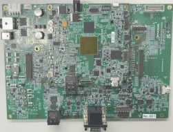
R-Car V4H 系统评测板套装 / White Hawk
White Hawk 是一款适用于 R-Car V4H 的评估套件,可使用 R-Car V4H 来评估系统并用来开发操作系统、设备驱动器和应用程序。 使用 White Hawk 评估套件可让开发人员高效地执行所需任务,例如评估 R-Car V4H 系统性能,从而大大缩短产品开发的周期。
该板支持多摄像头输入,包括4K高分辨率输入、4K 显示输出、音频输出、网络通信接口和适用于多 ECU 并行运行的 PCIe Gen4。
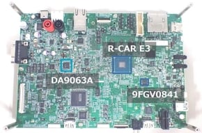
全图形仪表和驾驶舱解决方案 R-Car E3 开发板/Ebisu
R-Car E3 和时钟发生器的组合,为全图形仪表解决方案提供经过优化的功能及性能,为集成驾驶舱解决方案的大尺寸面板给予支持,其常见于入门级车型中。 开发人员可以使用该开发板评估 R-Car E3 系统级芯片(SoC)并着手开发软硬件解决方案。
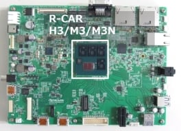
高端驾驶舱和信息娱乐系统解决方案 R-Car H3、M3 开发板/Salvator-XS
R-Car(H3/M3/M3N)系统级封装(SiP)和时钟发生器的组合可提供高效率,同时支持多种显示输出和高质量性能,因此十分适合可扩展的驾驶舱和信息娱乐系统解决方案。


