封装信息
| CAD 模型: | View CAD Model |
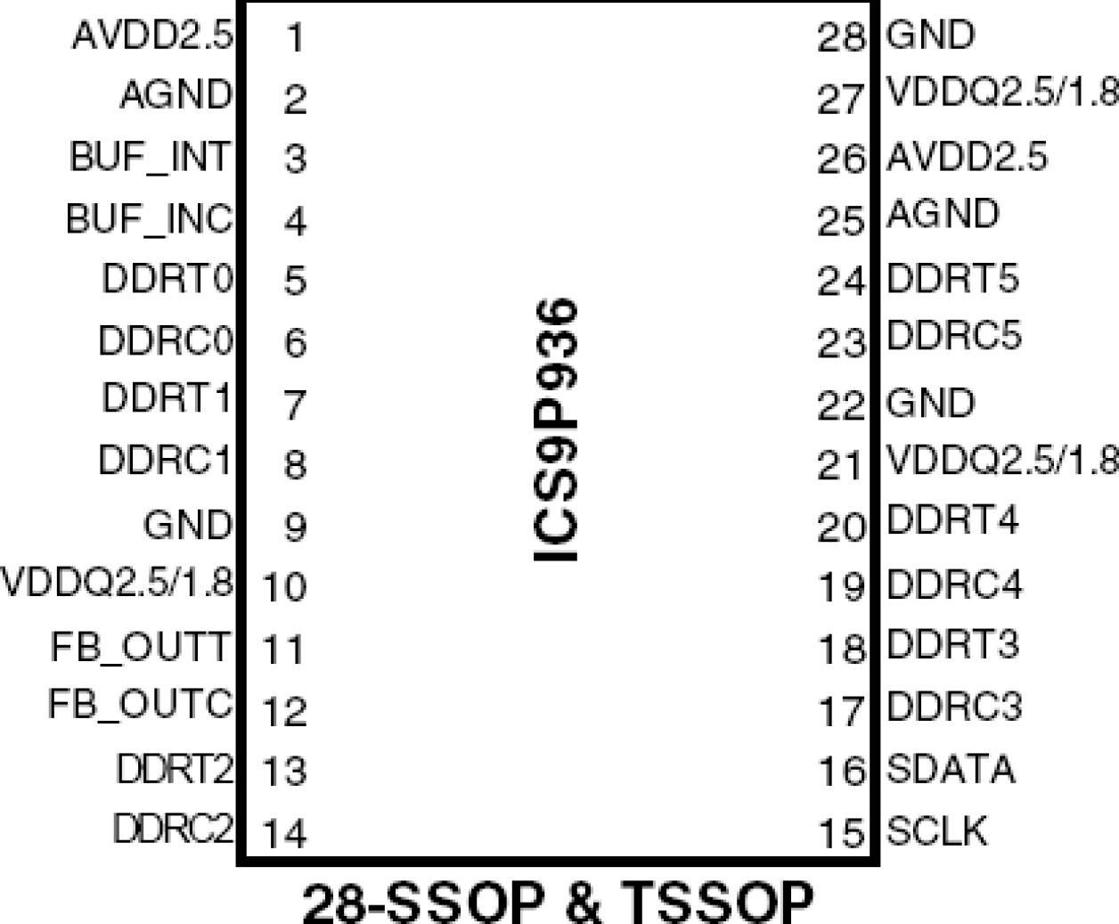
| Pkg. Type: | TSSOP |
| Pkg. Code: | PGG28 |
| Lead Count (#): | 28 |
| Pkg. Dimensions (mm): | 9.7 x 4.4 x 1.0 |
| Pitch (mm): | 0.65 |
环境和出口类别
| Moisture Sensitivity Level (MSL) | 1 |
| Pb (Lead) Free | Yes |
| ECCN (US) | EAR99 |
| HTS (US) | 8542.39.0090 |
产品属性
| Lead Count (#) | 28 |
| Carrier Type | Tube |
| Moisture Sensitivity Level (MSL) | 1 |
| Qty. per Reel (#) | 0 |
| Qty. per Carrier (#) | 50 |
| Package Area (mm²) | 42.7 |
| Pkg. Dimensions (mm) | 9.7 x 4.4 x 1.0 |
| Pb (Lead) Free | Yes |
| Pb Free Category | e3 Sn |
| Temp. Range (°C) | 0 to 70°C |
| Core Voltage (V) | 1.8V, 2.5V |
| Function | Buffer |
| Input Freq (MHz) | 45 - 500 |
| Input Type | LVCMOS |
| Inputs (#) | 1 |
| Length (mm) | 9.7 |
| MOQ | 2000 |
| Output Banks (#) | 1 |
| Output Freq Range (MHz) | 45 - 500 |
| Output Skew (ps) | 40 |
| Output Type | LVCMOS |
| Output Voltage (V) | 1.8V, 2.5V |
| Outputs (#) | 6 |
| Pitch (mm) | 0.65 |
| Pkg. Type | TSSOP |
| Product Category | Clock Buffers & Drivers |
| Requires Terms and Conditions | Does not require acceptance of Terms and Conditions |
| Tape & Reel | No |
| Thickness (mm) | 1 |
| Width (mm) | 4.4 |
有关 9P936 的资源
描述
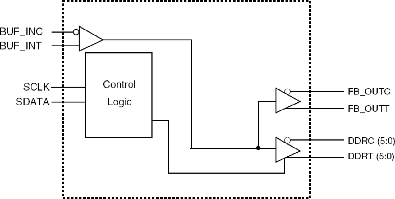
Dual DDR I/II fanout buffer for VIA Chipset


