
特性
- 12-bit resolution
- 3.3 V LVCMOS compatible digital outputs
- 74 dB SFDR
- 66.5 dB S/N (fi = 175 MHz
- fclk = 80 MHz
- B = Nyquist)
- 90 dB SFDR
- 71 dB S/N (fi = 225 MHz
- fclk = 80 MHz
- B = 5 MHz)
- Binary or 2's-complement LVCMOS outputs
- CMOS compatible static digital inputs
- Differential input with 375 MHz bandwidth
- Full-scale controllable from 1.5 V to 2 V (p-p)
- continuous scale
- High speed sampling rate up to 80 MHz
- HTQFP48 package
- Industrial temperature range from -40°C to +85°C
- Internal front-end buffer (input capacitance <1 pF)
- Only 2 clock cycles latency
- Programmable acquisition output clock (complete conversion signal)
- Single 5 V power supply
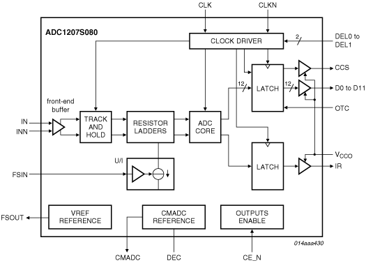
ADC1207S080HW - Block Diagram
描述
The ADC1207S080 is a 12-bit Analog-to-Digital Converter (ADC) optimized for direct Input Frequency (IF) sampling and supporting the most demanding use conditions in ultra high IF radio transceivers for cellular infrastructure and other applications such as wireless infrastructure, optical networking and fixed telecommunication. Due to its broadband input capabilities, the ADC1207S080 is ideal for single and multiple carriers data conversion. Operating at a maximum sampling rate of 80 MHz, analog input signals are converted into 12-bit binary coded digital words. All static digital inputs are CMOS compatible. All output signals are Low-Voltage Complementary Metal-Oxide Semiconductor (LVCMOS) compatible.


