特性
- High-voltage types (20V rating)
- Propagation delay time = 60ns (typ.) at CL = 50pF, VDD = 10V
- Buffered inputs and outputs
- Standard symmetrical output characteristics
- 100% tested for maximum quiescent current at 20V
- 5V, 10V and 15V parametric ratings
- Maximum input current of 1µA at 18V over full package temperature range; 100nA at 18V and +25 °C
- Noise margin (over full package temperature range):
- 1V at VDD = 5V
- 2V at VDD = 10V
- 2.5V at VDD = 15V
- Meets all requirements of JEDEC tentative standards No. 13B, "Standard Specifications for Description of "B" Series CMOS Device's
描述
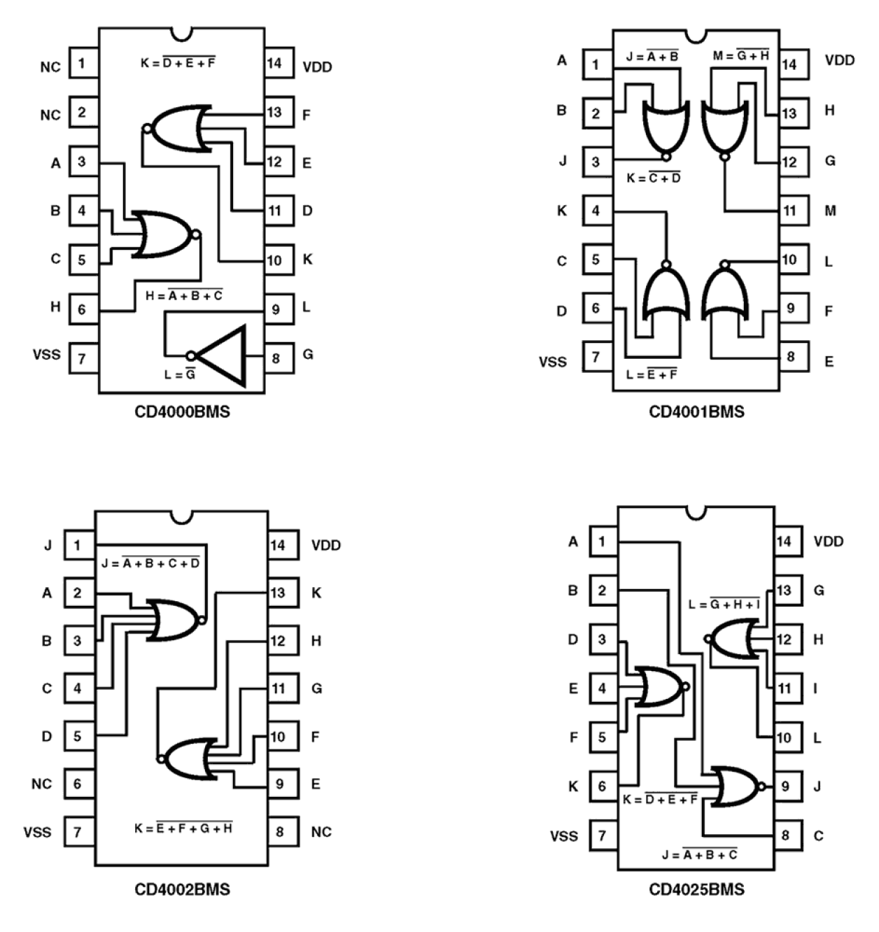
The CD4000BMS (dual 3 plus inverter), CD4001BMS (quad 2-input), CD4002BMS (dual 4-input), and CD4025BMS (triple 3-input) NOR gates provide the system designer with direct implementation of the NOR function and supplement the existing family of CMOS gates. All inputs and outputs are buffered. The CD4000BMS, CD4001BMS, CD4002BMS, and the CD4025BMS are supplied in these 14-lead outline packages: Braze Seal DIP H4X and H4Q, Frit Seal DIP H1B, and Ceramic Flatpack H3W.
当前筛选条件

