
特性
- 9 LVCMOS Compatible Clock Outputs
- 2 Selectable, LVCMOS Compatible Inputs
- Maximum Clock Frequency of 350 MHz
- Maximum Clock Skew of 150 ps
- Synchronous Output Stop in Logic Low State Eliminates Output Runt Pulses
- High-Impedance Output Control
- 3.3 V or 2.5 V Power Supply
- Drives up to 18 Series Terminated Clock Lines
- Ambient Temperature Range -40°C to +85°C
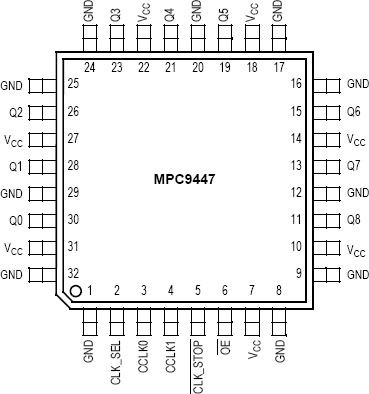
- 32-Lead LQFP Packaging
- 32-lead Pb-free Package Available
- Supports Clock Distribution in Networking, Telecommunications, and Computer Applications
- Pin and Function Compatible to MPC947
描述
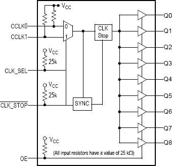
MPC9447 is specifically designed to distribute LVCMOS compatible clock signals up to a frequency of 350 MHz. Each output provides a precise copy of the input signal with a near zero skew. The outputs buffers support driving of 50 ? terminated transmission lines on the incident edge. Each is capable of driving either one parallel terminated or two series terminated transmission lines. Two selectable independent LVCMOS compatible clock inputs are available, providing support of redundant clock source systems. The MPC9447 CLK_STOP control is synchronous to the falling edge of the input clock. It allows the start and stop of the output clock signal only in a logic low state, and thus, eliminates potential output runt pulses. Applying the OE control will force the outputs into high-impedance mode. All inputs have an internal pull-up or pull-down resistor preventing unused and open inputs from floating. The device supports a 2.5 V or 3.3 V power supply and an ambient temperature range of -40°C to +85°C. The MPC9447 is pin and function compatible but performance-enhanced to the MPC947.