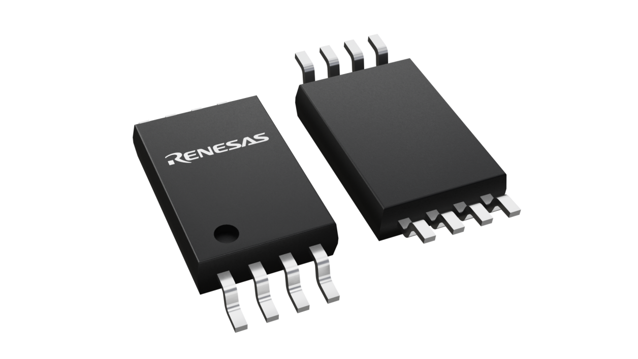
封装信息
| CAD 模型: | View CAD Model |
| Pkg. Type: | TSSOP |
| Pkg. Code: | pkg_8307 |
| Lead Count (#): | 8 |
| Pkg. Dimensions (mm): | 4.4 x 3.15 x 1.2 |
| Pitch (mm): | 0.65 |
环境和出口类别
| Moisture Sensitivity Level (MSL) | |
| Pb (Lead) Free | Yes |
| ECCN (US) | EAR99 |
| HTS (US) | 8542.33.0001 |
| RoHS (READ2302GSP#GC0) | 英语日文 |
产品属性
| Lead Count (#) | 8 |
| Pb (Lead) Free | Yes |
| Bandwidth (MHz) | 6 |
| CMRR (dB) | 80 |
| Channels (#) | 2 |
| Common Mode Input Voltage Range (V) | VSS - VDD |
| IBIAS (nA) | 0.001 |
| IS per Amp (mA) | 0.75 |
| Input Offset Voltage Vio (Max) (mV (±)) | 6 |
| Lead Compliant | Yes |
| Length (mm) | 4 |
| MOQ | 2500 |
| Output Voltage Swing Range (V) | VSS+0.2 - VDD-0.2 |
| PSRR (db) | 80 |
| Pkg. Dimensions (mm) | 4 x 3 x 1.2 |
| Pkg. Type | TSSOP |
| Process | CMOS |
| Qualification Level | Standard |
| Rail-to-Rail Input | Yes |
| Rail-to-Rail Output | Yes |
| Single Supply Voltage Range (V) | 2.5 - 5.5 |
| Slew Rate (V/µs) | 8 |
| Tape & Reel | No |
| Thickness (mm) | 1.2 |
| VS (Max) (V) | 6.5 |
| Width (mm) | 3 |
| field__slew_rate_typical_ | 8 |
有关 READ2302G 的资源
描述
The READ2302G is input and output full range dual CMOS Operational Amplifier realizing high drivability and high slew rate. This IC can be used in minimum operating supply voltage from 2. 5V, and in wide ambient temperature range from -40°C to +105°C. Available in ultra-small 8 pins TSSOP packages.
